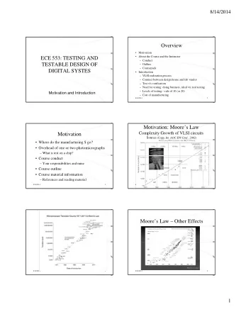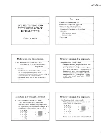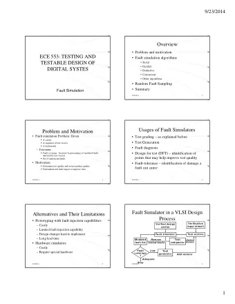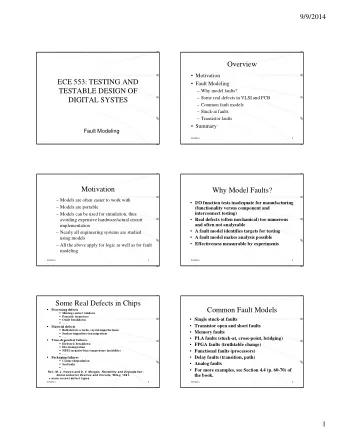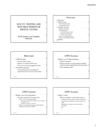
ECE 553: TESTING AND Partial-scan architecture TESTABLE DESIGN OF - PDF document
11/18/2014 Overview: Partial-Scan & Scan Variations Definition ECE 553: TESTING AND Partial-scan architecture TESTABLE DESIGN OF Scan flip-flop selection methods Cyclic and acyclic structures Cyclic and acyclic structures
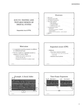
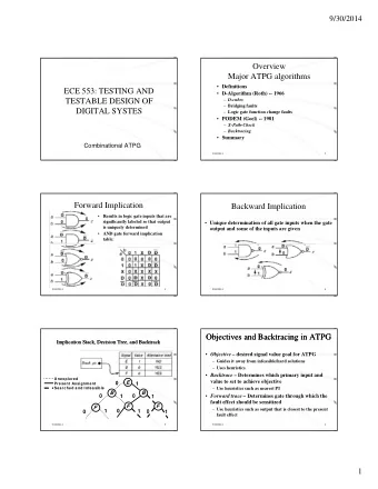
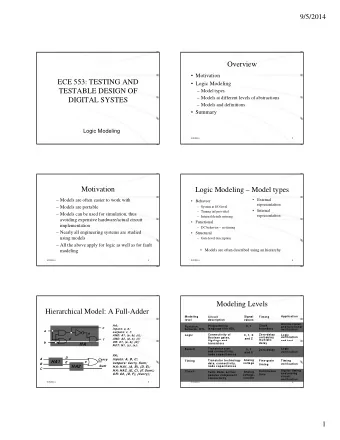
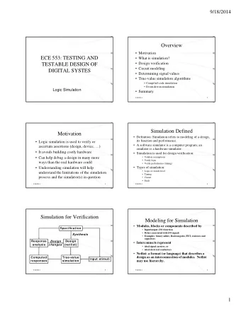
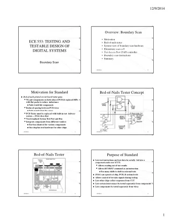
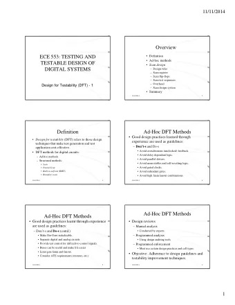
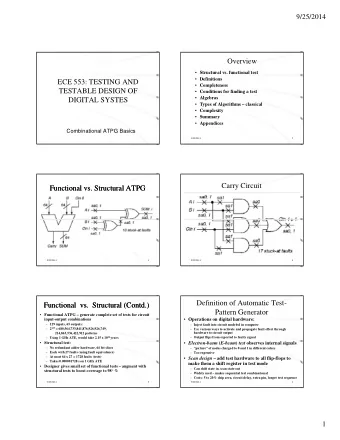
11/18/2014 Overview: Partial-Scan & Scan Variations • Definition ECE 553: TESTING AND • Partial-scan architecture TESTABLE DESIGN OF • Scan flip-flop selection methods • Cyclic and acyclic structures Cyclic and acyclic structures DIGITAL SYSTEMS DIGITAL SYSTEMS • Partial-scan by cycle-breaking • Scan variations • Scan-hold flip-flop (SHFF) • Summary Design for Testability (DFT) - 2 11/18/2014 2 Partial-Scan Architecture Partial-Scan Definition • A subset of flip-flops is scanned. PI PO • Objectives: Combinational circuit – Minimize area overhead and scan sequence length, yet achieve required fault coverage – Exclude selected flip-flops from scan: Exclude selected flip flops from scan: CK1 CK1 • Improve performance FF • Allow limited scan design rule violations FF – Allow automation: CK2 SCANOUT • In scan flip-flop selection SFF • In test generation TC – Shorter scan sequences SFF SCANIN 11/18/2014 3 11/18/2014 4 Cycle Breaking Scan Flip-Flop Selection Methods • Difficulties in ATPG • Testability measure based – Use of SCOAP: limited success. • S-graph and MFVS problem • Structure based: • Test generation and test statistics – Cycle breaking C l b ki • Partial vs. full scan – Balanced structure • Partial-scan flip-flop • Sometimes requires high scan percentage • ATPG based: – Use of combinational and sequential TG 11/18/2014 5 11/18/2014 6 1
11/18/2014 Difficulties in Seq. ATPG Benchmark Circuits • Poor initializability. Circuit s1196 s1238 s1488 s1494 PI 14 14 8 8 • Poor controllability/observability of state variables. PO 14 14 19 19 FF 6 18 18 6 • Gate count, number of flip-flops, and sequential Gates 508 647 529 653 Structure Cycle-free Cycle-free Cyclic Cyclic depth do not explain the problem. p p p Sequential depth Sequential depth 4 4 4 4 -- -- Total faults 1242 1355 1486 1506 • Cycles are mainly responsible for complexity. Detected faults 1239 1283 1384 1379 Circuit Number of Number of Sequential ATPG Fault Potentially detected faults 0 0 2 2 • An ATPG experiment: gates flip-flops depth CPU s coverage Untestable faults 3 72 26 30 Abandoned faults 0 0 76 97 TLC 355 21 14* 1,247 89.01% Fault coverage (%) 99.8 94.7 93.1 91.6 Fault efficiency (%) 100.0 100.0 94.8 93.4 Chip A 1,112 39 14 269 98.80% Max. sequence length 3 3 24 28 Total test vectors 313 308 525 559 * Maximum number of flip-flops on a PI to PO path 11/18/2014 7 11/18/2014 8 Cycle-Free Example Relevant Results Circuit • Theorem 8.1: A cycle-free circuit is always F2 initializable. It is also initializable in the presence 2 of any non-flip-flop fault. F3 F3 • Theorem 8 2: Any non flip flop fault in a cycle • Theorem 8.2: Any non-flip-flop fault in a cycle- F1 free circuit can be detected by at most d seq + 1 3 Level = 1 F2 vectors. 2 • ATPG complexity: To determine that a fault is s - graph untestable in a cyclic circuit, an ATPG program F1 F3 d seq = 3 using nine-valued logic may have to analyze 9 Nff Level = 1 3 time-frames, where Nff is the number of flip-flops All faults are testable. See Example 8.6. in the circuit. 11/18/2014 9 11/18/2014 10 The MFVS Problem A Partial-Scan Method • For a directed graph find a set of vertices with smallest cardinality such that the deletion of this vertex-set makes the graph acyclic. • Select a minimal set of flip-flops for scan to • The minimum feedback vertex set (MFVS) problem is NP- eliminate all cycles. complete; practical solutions use heuristics. • Alternatively, to keep the overhead low only long • A secondary objective of minimizing the depth of acyclic graph is useful. graph is useful cycles may be eliminated. cycles may be eliminated • In some circuits with a large number of self-loops, 3 all cycles other than self-loops may be eliminated. 3 L=3 1 2 4 5 6 1 2 4 5 6 L=2 L=1 s-graph A 6-flip-flop circuit 11/18/2014 11 11/18/2014 12 2
11/18/2014 Test Generation Partial Scan Example • Scan and non-scan flip-flops are controlled from • Circuit: TLC separate clock PIs: • 355 gates • Normal mode – Both clocks active • 21 flip-flops • Scan mode – Only scan clock active Scan Max. cycle Depth* Fault ATPG Test seq. • Seq. ATPG model: flip-flops length cov. vectors length • Scan flip-flops replaced by PI and PO S fli fl l d b PI d PO 0 4 14 89.01% 805 805 • Seq. ATPG program used for test generation • Scan register test sequence, 001100…, of length n sff + 4 applied in 4 2 10 95.90% 247 1,249 the scan mode 9 1 5 99.20% 136 1,382 • Each ATPG vector is preceded by a scan-in sequence to set scan flip-flop states 10 1 3 100.00% 112 1,256 • A scan-out sequence is added at the end of each vector sequence 21 0 0 100.00% 52 1,190 • Test length = (n ATPG + 2) n sff + n ATPG + 4 clocks * Cyclic paths ignored 11/18/2014 13 11/18/2014 14 Flip-flop for Partial Scan Partial vs. Full Scan: S5378 • Normal scan flip-flop (SFF) with multiplexer of the LSSD flip- flop is used. Original Partial-scan Full-scan • Scan flip-flops require a separate clock control: Number of combinational gates 2,781 2,781 2,781 • Either use a separate clock pin Number of non-scan flip-flops 179 149 0 • Or use an alternative design for a single clock pin (10 gates each) 0 179 Number of scan flip-flops 30 D Master Slave (14 gates each) MUX Q Gate overhead 0.0% 2.63% 15.66% latch latch SD Number of faults 4,603 4,603 4,603 PI/PO for ATPG 35/49 65/79 214/228 TC Fault coverage 70.0% 93.7% 99.1% SFF CK Fault efficiency 70.9% 99.5% 100.0% (Scan flip-flop) Number of ATPG vectors 414 1,117 585 TC Scan sequence length 414 34,691 105,662 CK Normal mode Scan mode 11/18/2014 15 11/18/2014 16 Scan Set Scan Variations • Integrated and Isolated scan methods PI PO Logic – Scan path: NEC 1968 And Flip-flops – Serial scan: 1973 – LSSD: IBM 1977 LSSD: IBM 1977 CK CK – Scan set: Univac 1977 TC SCANOUT – RAS: Fujitsu/Amdahl 1980 SCANIN 11/18/2014 17 11/18/2014 18 3
11/18/2014 Random-Access Scan (RAS) Scan Set Applications • Advantages PI PO Combinational – Potentially useable in delay testing. logic RAM – Concurrent testing: can sample the system state Concurrent testing: can sample the system state n ff while the system is running CK bits • Used in microrollback TC SCANIN SCANOUT • Disadvantages SEL Address decoder – Higher overhead due to routing difficulties Address scan ADDRESS register ACK log 2 n ff bits 11/18/2014 19 11/18/2014 20 RAS Flip-Flop (RAM Cell) RAS Applications • Logic test: reduced test length. D Q From comb. logic To comb. • Delay test: Easy to generate single-input-change logic SD Scan flip-flop SCANIN (SFF) (SIC) delay tests. • Advantage: RAS may be suitable for certain Ad RAS b i bl f i CK architecture, e.g., where memory is implemented TC as a RAM block. SCANOUT • Disadvantages: SEL • Not suitable for random logic architecture • High overhead – gates added to SFF, address decoder, address register, extra pins and routing – BUT these are addressed by Dong Baik in his Ph.D. work (ITC 2005). 11/18/2014 21 11/18/2014 22 Scan-Hold Flip-Flop (SHFF) To SD of next SHFF D Q SD SFF TC Q C CK HOLD • The control input HOLD keeps the output steady at previous state of flip-flop. • Applications: • Reduce power dissipation during scan • Isolate asynchronous parts during scan test • Delay testing 11/18/2014 23 11/18/2014 24 4
11/18/2014 Summary • Partial-scan is a generalized scan method; scan can vary from 0 to 100%. • Elimination of long cycles can improve testability via sequential ATPG. • Elimination of all cycles and self-loops allows combinational ATPG. • Partial-scan has lower overheads (area and delay) and reduced test length. • Partial-scan allows limited violations of scan design rules, e.g., a flip-flop on a critical path may not be scanned. 11/18/2014 25 5
Recommend
More recommend
Explore More Topics
Stay informed with curated content and fresh updates.
