Overview Motivation ECE 553: TESTING AND Logic Modeling - - PDF document

overview
SMART_READER_LITE
LIVE PREVIEW

Overview Motivation ECE 553: TESTING AND Logic Modeling - - PDF document

9/5/2014 Overview Motivation ECE 553: TESTING AND Logic Modeling TESTABLE DESIGN OF Model types Models at different levels of abstractions Models at different levels of abstractions DIGITAL SYSTES DIGITAL SYSTES


slide-1
SLIDE 1

9/5/2014 1

ECE 553: TESTING AND TESTABLE DESIGN OF DIGITAL SYSTES DIGITAL SYSTES
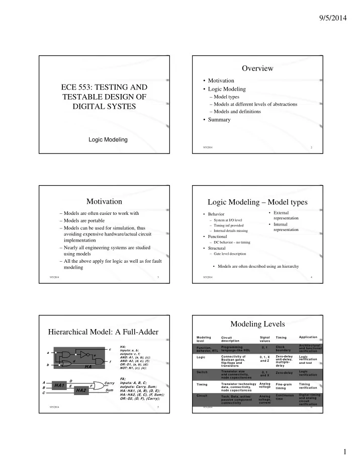
Logic Modeling

Overview

  • Motivation
  • Logic Modeling

– Model types – Models at different levels of abstractions

9/5/2014 2

– Models at different levels of abstractions – Models and definitions

  • Summary

Motivation

– Models are often easier to work with – Models are portable – Models can be used for simulation, thus avoiding expensive hardware/actual circuit

9/5/2014 3

avoiding expensive hardware/actual circuit implementation – Nearly all engineering systems are studied using models – All the above apply for logic as well as for fault modeling

Logic Modeling – Model types

  • Behavior

– System at I/O level – Timing inf provided – Internal details missing

  • External

representation

  • Internal

representation

9/5/2014 4

  • Functional

– DC behavior – no timing

  • Structural

– Gate level description

  • Models are often described using an hierarchy

Hierarchical Model: A Full-Adder

HA; inputs: a, b;

  • utputs: c, f;

AND: A1, (a, b), (c); AND: A2, (d, e), (f); OR: O1 (a b) (d);

a b c d e f

9/5/2014 5

OR: O1, (a, b), (d); NOT: N1, (c), (e);

b

HA

FA; inputs: A, B, C;

  • utputs: Carry, Sum;

HA: HA1, (A, B), (D, E); HA: HA2, (E, C), (F, Sum); OR: O2, (D, F), (Carry);

HA1 HA2

A B C D E F Sum Carry

Modeling Levels

Circuit description Programming language-like HDL Connectivity of Boolean gates, flip-flops and Signal values 0, 1 0, 1, X and Z Timing Clock boundary Zero-delay unit-delay, multiple- Modeling level Function, behavior, RTL Logic Application Architectural and functional verification Logic verification and test

9/5/2014 6

p p transistors Transistor size and connectivity, node capacitances Transistor technology data, connectivity, node capacitances

  • Tech. Data, active/

passive component connectivity 0, 1 and X Analog voltage Analog voltage, current delay Zero-delay Fine-grain timing Continuous time Sw itch Timing Circuit Logic verification Timing verification Digital timing and analog circuit verification

slide-2
SLIDE 2

9/5/2014 2

Logic Models and definitions*

  • Combinational circuit models

– Function expressed as truth-table or cubes – Cubes and cube intersection can be used during simulation

  • Sequential Circuits

9/5/2014 7

– Structure represented as a collection of flip-flops feeding combinational logic – Time frame expansion is possible

  • Binary Decision Diagrams (BDD)

*Ref: Abramovici et. al, Digital system testing and testable design Logic Models and definitions (2)

  • Program model of a circuit

– Express circuit (gate level) as a program consisting of interconnected logic operations – Execute the program to determine circuit output for varying inputs

9/5/2014 8

inputs

  • RTL model

– Higher level model of the circuit

  • HDL model

– Examples at this level are verilog HDL and VHDL

Logic Models and definitions (3)

  • Structural model

– External representation in the form of netlist – Examples of this are uw format, iscas format, EDIF, … – Some keywords used in such representation

  • Primary inputs and Primary outputs

9/5/2014 9

  • Gates: AND, OR, NOT, …
  • Storage: latch, flip-flop
  • Connections: lines, nets
  • Fanin: number of inputs to a gate
  • Fanout: number of lines a signal feeds
  • Fanoutfree circuit: every line or gate has a fanout of one

Netlist Format: Two Examples

UW format

# gate connected to 1 PI 4, 5 ; 2 PI 3 6

  • utput = gate(inputs)

INPUT(G1) INPUT(G2)

ISCAS format

9/5/2014 10

2 PI 3, 6 ; 3 not 5 ; 4 not 6 ; 5 and 7 ; 6 and 7 ; 7 or 8 ; 8 PO ; INPUT(G2) OUTPUT(G7) G3 = NOT(G2) G4 = NOT(G1) G5 = AND(G1, G3) G6 = AND(G2, G4) G7 = OR(G5, G6)

Logic Models and definitions (4)

  • Structural model

– Internal representation in the form of tables

  • Tables of gates and storage elements (names)
  • Tables of connections

9/5/2014 11

  • Tables of fanin and fanouts

– Objective is to make the storage and search processes (integral part of simulation) more efficient – Knowledge of data structures and algorithms is very useful

Logic Models and definitions (5)

  • Additional useful terms

– Graph representation – Reconvergent fanouts – Stems and branches

9/5/2014 12

Stems and branches – Logic levels in a circuit – “levelization” of a circuit

slide-3
SLIDE 3

9/5/2014 3

Summary

  • Modeling of logic circuit offers many advantages
  • Many modeling levels exist and are used
  • Gate level models are most prevalent in logic testing

9/5/2014 13