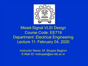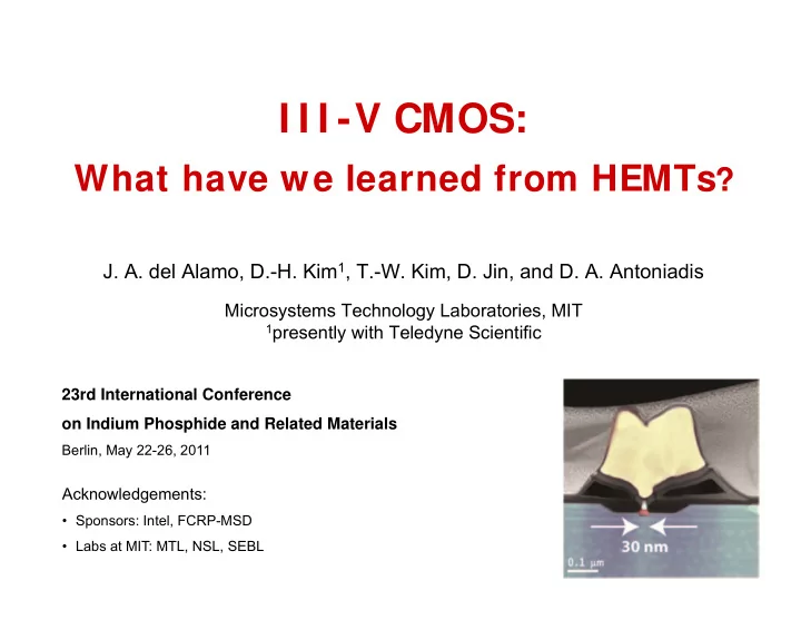
I I I -V CMOS: What have we learned from HEMTs ? J. A. del Alamo, - PowerPoint PPT Presentation
I I I -V CMOS: What have we learned from HEMTs ? J. A. del Alamo, D.-H. Kim 1 , T.-W. Kim, D. Jin, and D. A. Antoniadis Microsystems Technology Laboratories, MIT 1 presently with Teledyne Scientific 23rd International Conference on Indium
I I I -V CMOS: What have we learned from HEMTs ? J. A. del Alamo, D.-H. Kim 1 , T.-W. Kim, D. Jin, and D. A. Antoniadis Microsystems Technology Laboratories, MIT 1 presently with Teledyne Scientific 23rd International Conference on Indium Phosphide and Related Materials Berlin, May 22-26, 2011 Acknowledgements: • Sponsors: Intel, FCRP-MSD • Labs at MIT: MTL, NSL, SEBL 1
Outline • Why III-Vs for CMOS? • What have we learned from III-V HEMTs • III-V CMOS device design and challenges • Conclusions 2
CMOS scaling in the 21 st century • Si CMOS has entered era of “power-constrained scaling”: – Microprocessor power density saturated at ~100 W/cm 2 – Microprocessor clock speed saturated at ~ 4 GHz Intel microprocessors Pop, Nano Res 2010 3
Consequences of Power Constrained Scaling Power = active power + stand-by power 2 N N ↑ V DD ↓ P A ~ f CV DD clock frequency #1 goal! transistor capacitance operating voltage transistor count Transistor scaling requires reduction in supply voltage Not possible with Si: performance degrades too much 4
How I I I -Vs allow further V DD reduction? • Goals of scaling: – reduce transistor footprint – extract maximum I ON for given I OFF 5
How I I I -Vs allow further V DD reduction? • Goals of scaling: – reduce transistor footprint – extract maximum I ON for given I OFF • III-Vs: – higher electron velocity than Si I ON ↑ – tight carrier confinement in quantum well S ↓ V DD ↓ 6
What have we learned from I I I -V HEMTs? State-of-the-art: InAs HEMTs Gate S D Oxide - QW channel (t ch = 10 nm): Cap • InAs core (t InAs = 5 nm) Etch stopper Barrier t ins • InGaAs cladding t ch n,Hall = 13,200 cm 2 /V-sec Channel - Buffer - InAlAs barrier (t ins = 4 nm) - Ti/Pt/Au Schottky gate - L g =30 nm Kim, EDL 2010 7 7
L g = 30 nm I nAs HEMT Kim, EDL 2010 2.0 V GS = 0.8 0.4 V 1.5 0.6 g m [mS/ m] I D [mA/ m] 0.2 V 1.0 0.4 0.5 0.2 0 V V DS = 0.5 V 0.0 0.0 0.0 0.2 0.4 0.6 0.8 -0.6 -0.4 -0.2 0.0 0.2 V DS [V] V GS [V] • Large current drive: I ON >0.5 mA/µm at V DD =0.5 V • V T = -0.15 V, R S =190 ohm. μ m • High transconductance: g mpk = 1.9 mS/ μ m at V DD =0.5 V 8 8 8
L g = 30 nm I nAs HEMT Kim, EDL 2010 40 3 -3 10 V DS = 0.5 V H 21 -4 10 30 2 U g f T = 644 GHz V DS = 0.05 V I D -5 10 Gains [dB] f max = 681 GHz I D , I G [A/ m] MSG/MAG 20 1 -6 10 K V DS = 0.5 V -7 10 10 0 K I G -8 10 V DS =0.5 V, V GS =0.2 V V DS = 0.05 V -9 10 0 -1 -1.0 -0.8 -0.6 -0.4 -0.2 0.0 0.2 0.4 9 10 11 12 10 10 10 10 V GS [V] Frequency [Hz] • Only transistor of any kind with both f T and f max > 640 GHz • S = 74 mV/dec, DIBL = 80 mV/V, I on /I off ~ 5x10 3 • All FOMs at V DD =0.5 V 9 9
I nAs HEMTs: Benchmarking with Si • FOM that integrates short-channel effects and transport: I ON @ I OFF =100 nA/µm, V DD =0.5 V IEDM 2008 InAs HEMTs: higher I ON for same I OFF than Si: Why? 10
Why high I ON ? 1. Very high electron injection velocity at the virtual source v inj E C E V Kim, IEDM 2009 Liu, Springer 2010 • v inj (InGaAs) increases with InAs fraction in channel • v inj (InGaAs) > 2v inj (Si) at less than half V DD • ~100% ballistic transport at L g ~30 nm 11
Why high I ON ? 2. Quantum capacitance less of a bottleneck than previously believed InAs channel: t ch = 10 nm 40 Experiment (C G ) C ins ( t ins = 4 nm) Capacitance [fF/ m 2 ] 30 C Q1 (m ||* = 0.026m e ) 20 C cent1 C G ( 0.07 ) 10 C G ( 0.05 ) C G (m ||* = 0.026m e ) Jin, IEDM 2009 0 -0.4 -0.2 0 0.2 0.4 V G [V] Biaxial strain + non-parabolicity + strong quantization: m || * ↑ C G ↑ n s ↑ I ON ↑ 12
Why high I ON ? 3. Sharp subthreshold swing due to quantum-well channel state-of-the-art Si 90 In 0.7 Ga 0.3 As HEMTs: t ch = 13 nm Subtreshold swing [mV/dec] 80 InAs HEMTs: t ch = 10 nm 70 InAs HEMTs: t ch = 5 nm t ins = 4 nm, L side = 80 nm 60 Kim, IPRM 2010 40 80 120 160 200 L g [nm] • Dramatic improvement in short-channel effects with thin channel • Thin channel does not degrade v inj at L g ~40 nm (Kim, IPRM 2011) 13
Limit to I I I -V HEMT Scaling: Gate Leakage Current -3 InAs HEMT 10 t ins = 10 nm L g = 30 nm t ins = 7 nm -4 10 I D t ins = 4 nm t ch = 10 nm -5 10 t ins =4 nm I D , I G [A/ m] -6 10 I G -7 10 t ins =7 nm -8 10 -9 t ins =10 nm 10 V DS = 0.5 V -10 10 -1.00 -0.75 -0.50 -0.25 0.00 0.25 0.50 V GS [V] t ins ↓ I G ↑ Further scaling requires high-K gate dielectric 14 14
I I I -V CMOS: device design and challenges Modern III-V HEMT vs. modern Si MOSFET: Intel’s 45 nm CMOS III-V HEMT ~2 m • What do we preserve? • What do we change? 15
I I I -V CMOS: HEMT features worth preserving • Quantum-well channel: key to scalability • Undoped channel: • InAs-rich channel: for high mobility and velocity • Buried-channel design: • Raised source and drain regions: essential for scalability • Undoped QW channel in extrinsic regions: key to low access resistance 16
I I I -V CMOS: HEMT features to change • Schottky gate: need MOS gate with very thin high-K dielectric • T-gate: need rectangular gate • Barrier under contacts: need to eliminate • Alloyed ohmic contacts: change to refractory ohmic contacts • Source and drain contacts: need self-aligned with gate • Footprint: need to reduce by 1000 X! n + n + HEMT QW-MOSFET 17
I I I -V CMOS: other critical needs • p-channel MOSFET: with performance >1/3 that of n-MOSFET • Co-integration of n-FET and p-FET on Si: compact, planar surface n-MOSFET p-MOSFET Silicon 18
I I I -V CMOS: other designs n + n + Etched S/D QW-MOSFET Regrown S/D QW-MOSFET Gate-all-around FinFET nanowire FET 19
The high-water mark: I ntel’s I nGaAs Quantum-Well MOSFET Radosavljevic, IEDM 2009 Direct MBE on Si substrate (1.5 m buffer thickness) • • InGaAs buried-channel MOSFET (under 2 nm InP barrier) • 4 nm TaSiO x gate dielectric by ALD, L g =75 nm • First III-V QW-MOSFET with better performance than Si 20
More recent notable work XOI InAs MOSFET G S InAs D SiO 2 Si InAs Nanoribbon MOSFETs Aspect Ratio Trapping on Insulator (UC Berkeley) (Amberwave) Self-aligned QW-FET (MIT) Ko, Nature 2010 Fiorenza, ECS 2010 Kim, IEDM 2010 Gate Gate Source Source Drain Drain Fin-Channel Fin-Channel Fin-Channel Fin-Channel Fin-Channel Fin-Channel EXT. EXT. Fin-channel Fin-channel p InP p InP p+ InP p+ InP Al 2 O 3 /InGaSb QW- Ge p-type QW-MOSFET InGaAs FinFET (Purdue, Intel) MOSFET (Stanford) (Intel) Wu, IEDM 2009 Nainani, IEDM 2010 Pillarisetty, IEDM 2010 Radosavljevic, IEDM 2010 21
Conclusions • III-V HEMTs suggest strong potential for III-V CMOS: – InAs electron injection velocity > 2x that of Si at 1/2x V DD – Quantum capacitance less of a bottleneck than previously believed – Quantum-well channel yields outstanding short-channel effects • Impressive recent progress on III-V CMOS – Sub-100 nm InGaAs MOSFETs with I ON > than Si at 0.5 V demonstrated • Lots of work ahead – Demonstrate ~10 nm III-V N-MOSFET that is better than Si – P-channel MOSFET – N-channel + P-channel cointegration on Si 22
Recommend
More recommend
Explore More Topics
Stay informed with curated content and fresh updates.
