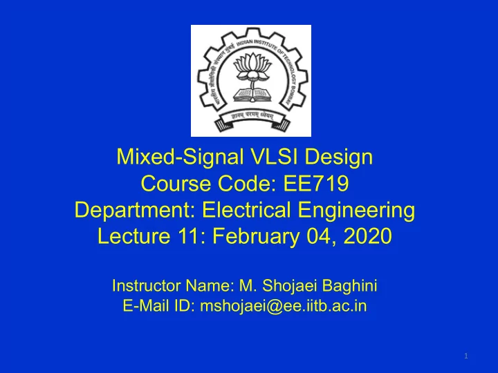
Mixed-Signal VLSI Design Course Code: EE719 Department: Electrical - PowerPoint PPT Presentation
Mixed-Signal VLSI Design Course Code: EE719 Department: Electrical Engineering Lecture 11: February 04, 2020 Instructor Name: M. Shojaei Baghini E-Mail ID: mshojaei@ee.iitb.ac.in 1 2 2 Module 11 Introduction to the Comparators References
Mixed-Signal VLSI Design Course Code: EE719 Department: Electrical Engineering Lecture 11: February 04, 2020 Instructor Name: M. Shojaei Baghini E-Mail ID: mshojaei@ee.iitb.ac.in 1
2 2 Module 11 Introduction to the Comparators References - Prof. Boris Murmann’s slides from “VLSI Data Conversion Circuits”, Stanford University, 2013. - Section “Latched Comparators” onwards from chapter “Comparators”, Analog Integrated Circuit Design by T. C. Carusone, D. A. Johns and K. Martin, J. Wiley & Sons, 2012. - “Clocked Comparator” from chapter “Submicron CMOS Circuit Design”, CMOS Mixed-signal Circuit Design by R. Jacob Baker, Wiley India, IEEE press, reprint 2009. - “Comparator” from chapter “Nonlinear Analog Circuits”, CMOS Circuit Design, Layout and Simulation by R. Jacob Baker, Wiley India, IEEE press, 2008. - “The StrongArm Latch”, B. Razavi, IEEE Solid-State Circuits Magazine, Spring 2015. IIT-Bombay Lecture 11 M. Shojaei Baghini
3 3 Ideal Voltage Comparator Infinite gain! - High gain but not necessarily linear amplification - Amplification can happen in discrete time. - Clocked versus un-clocked comparator IIT-Bombay Lecture 11 M. Shojaei Baghini
4 4 Realization of High Gain Operation - Common Technique for Amplifiers: Cascade of Stages - Amplification can happen in the form of a regenerative process due to positive feedback IIT-Bombay Lecture 11 M. Shojaei Baghini
5 5 Cascade of Gain Stages R R g m N: Optimal number of stages A v0 = -g m × R , A v = (A v0 ) N , BW 0 = ! "# = ! A v0 $ % where & ' = # ! $ = ( ) and C is the equivalent C observed at the output of each stage. ∆+ ,-. 1 2 V out (s) = V in (s)A v (s) = × 5 / 4 5 $ % / !31 2 IIT-Bombay Lecture 11 M. Shojaei Baghini
6 6 Step Response of the Multi-stage Amplifier with A v =10 Optimal number: N=3 B. Murmann’s course, Stanford univ., 2013 IIT-Bombay Lecture 11 M. Shojaei Baghini
7 7 How does minimum delay change with increasing A v ? B. Murmann’s course, Stanford Univ., 2013 IIT-Bombay Lecture 11 M. Shojaei Baghini
8 8 Analytical Derivation of the Optimum N A v = (A v0 ) N , t d ≈ N × " u × A v0 = N × " u × # $ %/' % %/' - %/' = 0 ⇒ dt d /dN = 0 ⇒ # $ ' ) *+(# $ ) . # $ N opt ≈ *+(# $ ) , A v0 = e , t d,min ≈ *+(# $ ) × " u × e e ≈ 2.7 Similar to logic effort-based buffer design! IIT-Bombay Lecture 11 M. Shojaei Baghini
9 9 Improving the Performance of Each Stage Removing resistors helps to feed the entire current to the capacitors (i.e. only capacitive load as opposed to RC load). B. Murmann’s course, Stanford Univ., 2013 IIT-Bombay Lecture 11 M. Shojaei Baghini
10 10 Performance Improvement using Integrator There is no limit for the final output but practically supply voltages will limit it. B. Murmann’s course, Stanford Univ., 2013 IIT-Bombay Lecture 11 M. Shojaei Baghini
11 11 Module 12 Latch as a Comparator References - Prof. Boris Murmann’s slides from “VLSI Data Conversion Circuits”, Stanford University, 2013. - Section “Latched Comparators” onwards from chapter “Comparators”, Analog Integrated Circuit Design by T. C. Carusone, D. A. Johns and K. Martin, J. Wiley & Sons, 2012. - “Clocked Comparator” from chapter “Submicron CMOS Circuit Design”, CMOS Mixed-signal Circuit Design by R. Jacob Baker, Wiley India, IEEE press, reprint 2009. - “Comparator” from chapter “Nonlinear Analog Circuits”, CMOS Circuit Design, Layout and Simulation by R. Jacob Baker, Wiley India, IEEE press, 2008. - “The StrongArm Latch”, B. Razavi, IEEE Solid-State Circuits Magazine, Spring 2015. IIT-Bombay Lecture 11 M. Shojaei Baghini
12 12 Replacing Cascade of N Integrators with a V DD Closed Loop of Integrators ! 2 Latch (regenerative ! 1 ! 1 sense amplifier) V IP V IN C L ! 2 C L V SS • Each inverter is a G m module driving a capacitive load and hence behaves as an integrator. • A closed loop of two inverters is mimicking cascade of infinite number of integrators. IIT-Bombay Lecture 11 M. Shojaei Baghini
13 13 Latch as a Comparator " # ! = $ % !! Latch gain B. Murmann’s course, Stanford Univ., 2013 IIT-Bombay Lecture 11 M. Shojaei Baghini
14 14 Latch as a Comparator - Example B. Murmann’s course, Stanford Univ., 2013 IIT-Bombay Lecture 11 M. Shojaei Baghini
15 15 Linear Behavior of log(V diff (t)) versus t and Initial Condition B. Murmann’s course, Stanford Univ., 2013 IIT-Bombay Lecture 11 M. Shojaei Baghini
16 16 Analysis of Latch Delay " #$,&#'() T d,latch = ! latch ln " #$,* C ≈ a × WLC ox , 1<a<2 g m ≈ b × + C ox W/L × V GST , 0.5<b<1 (either NMOS or PMOS transistor) ⇒ ! latch ≈ d × L 2 /( + n × V GST ) where 1<d<4 Velocity saturation: ! latch ≈ a × L/v sat K. Martin’s book, 2012 • B. Murmann’s course, Stanford • Univ., 2013 IIT-Bombay Lecture 11 M. Shojaei Baghini
17 17 End of Lecture 11 IIT-Bombay Lecture 11 M. Shojaei Baghini
Recommend
More recommend
Explore More Topics
Stay informed with curated content and fresh updates.

