Switch-Less Frequency-Domain Multiplexing of GFET Sensors and - PowerPoint PPT Presentation
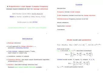
Switch-Less FDM GFET Sensors LP CMOS Frontend 1024-Ch ECOG Intro FDM ROIC CMOS Chip Conclusions Switch-Less Frequency-Domain Multiplexing of GFET Sensors and Low-Power CMOS Frontend for 1024-Channel ECOG J.Cisneros-Fernndez 1 , M.Dei
Switch-Less FDM GFET Sensors LP CMOS Frontend 1024-Ch µECOG Intro FDM ROIC CMOS Chip Conclusions Switch-Less Frequency-Domain Multiplexing of GFET Sensors and Low-Power CMOS Frontend for 1024-Channel µECOG J.Cisneros-Fernández 1 , M.Dei 1 , L.Terés 1,2 and F.Serra-Graells 1,2 jose.cisneros@imb-cnm.csic.es 1 Instituto de Microelectrónica de Barcelona, IMB-CNM(CSIC), Spain 2 Universitat Autònoma de Barcelona, Spain May 2019 J.Cisneros-Fernández, M.Dei, L.Terés and F.Serra-Graells
Switch-Less FDM GFET Sensors LP CMOS Frontend 1024-Ch µECOG Intro FDM ROIC CMOS Chip Conclusions 1/24 1 Introduction 2 Frequency-Domain Multiplexing of GFETs 3 1024-Ch ROIC Architecture 4 Low-Power CMOS Circuits 5 Test Chip in 0.18µm CMOS Technology 6 Conclusions J.Cisneros-Fernández, M.Dei, L.Terés and F.Serra-Graells
Switch-Less FDM GFET Sensors LP CMOS Frontend 1024-Ch µECOG Intro FDM ROIC CMOS Chip Conclusions 2/24 1 Introduction 2 Frequency-Domain Multiplexing of GFETs 3 1024-Ch ROIC Architecture 4 Low-Power CMOS Circuits 5 Test Chip in 0.18µm CMOS Technology 6 Conclusions J.Cisneros-Fernández, M.Dei, L.Terés and F.Serra-Graells
Switch-Less FDM GFET Sensors LP CMOS Frontend 1024-Ch µECOG Intro FDM ROIC CMOS Chip Conclusions 3/24 Introduction Low-power ICs with massive number of channels needed for neural recording Monolithical high density in small areas, high fabrication cost and low scalability . Hybrid (sensors+IC) device preferred for large sensing area, low cost, CMOS compatibility and fl exible substrates = sensor multiplexing Liquid-gate Graphene fi eld-e ff ect transistors ( GFETs ) are good candidates for micro-electrocorticography ( µECOG ) J.Cisneros-Fernández, M.Dei, L.Terés and F.Serra-Graells
Switch-Less FDM GFET Sensors LP CMOS Frontend 1024-Ch µECOG IntroFDM ROIC CMOS Chip Conclusions 4/24 1 Introduction 2 Frequency-Domain Multiplexing of GFETs 3 1024-Ch ROIC Architecture 4 Low-Power CMOS Circuits 5 Test Chip in 0.18µm CMOS Technology 6 Conclusions J.Cisneros-Fernández, M.Dei, L.Terés and F.Serra-Graells
Switch-Less FDM GFET Sensors LP CMOS Frontend 1024-Ch µECOG IntroFDM ROIC CMOS Chip Conclusions 5/24 Frequency-Domain Multiplexing Frequency-Domain Multiplexing Classic Time-Domain Multiplexing CMOS CMOS Column Column frontend frontend voltage digital carriers multiplexer Row Row current current Gfet read-out read-out Sensor Series Switch GFET matrix GFET matrix GFET + Switch technology integration Each GFET is permanently connected GFET mismatch + transient operation Switch-less and artifact-free =Multiplexing artifacs J.Cisneros-Fernández, M.Dei, L.Terés and F.Serra-Graells
Switch-Less FDM GFET Sensors LP CMOS Frontend 1024-Ch µECOG IntroFDM ROIC CMOS Chip Conclusions 6/24 Frequency-Domain Multiplexing Frequency-Domain Multiplexing Each GFET is permanently connected CMOS Column and used as transconductor + mixer frontend voltage carriers Carrier column Recording site voltage uecog signal Row current read-out Modulated GFET Current Irow di ff erent channels frequency allocation GFET matrix Insensitive to CMOS fl icker noise Low-noise lock-in demodulation J.Cisneros-Fernández, M.Dei, L.Terés and F.Serra-Graells
Switch-Less FDM GFET Sensors LP CMOS Frontend 1024-Ch µECOG IntroFDM ROIC CMOS Chip Conclusions 7/24 Frequency-Domain Multiplexing Symmetrical operation Asymmetrical operation GFET asymmetrical operation generates odd and even harmonics: FDM carrier pre-distortion to promote second-harmonic cancellation: + Calibration not needed + Compatible with I/Q generation J.Cisneros-Fernández, M.Dei, L.Terés and F.Serra-Graells
Switch-Less FDM GFET Sensors LP CMOS Frontend 1024-Ch µECOG IntroFDMROIC CMOS Chip Conclusions 8/24 1 Introduction 2 Frequency-Domain Multiplexing of GFETs 3 1024-Ch ROIC Architecture 4 Low-Power CMOS Circuits 5 Test Chip in 0.18µm CMOS Technology 6 Conclusions J.Cisneros-Fernández, M.Dei, L.Terés and F.Serra-Graells
Switch-Less FDM GFET Sensors LP CMOS Frontend 1024-Ch µECOG IntroFDMROIC CMOS Chip Conclusions 9/24 1024-Channel ROIC Architecture Modular and scalable read-out IC ( ROIC ) for 32x32 GFET sensory arrays: Dual Column Module (x16) ROIC Core supply DAC VCRO CP PFC columns of GFET array DAC Analog PLL voltage references Con fi g. Con fi guration Con fi g. Digital Bus control Con fi guration digital Preamp PGA Master backend clock I/O Bus rows of (e.g. lock-in Acquisition Bus GFET array demux) SAR ADC Analog Bias Row Module (x32) J.Cisneros-Fernández, M.Dei, L.Terés and F.Serra-Graells
Switch-Less FDM GFET Sensors LP CMOS Frontend 1024-Ch µECOG IntroFDMROIC CMOS Chip Conclusions 10/24 1024-Channel ROIC Architecture ROIC speci fi cations from functional model in Scienti fi c Python: Recording of local fi eld potentials ( LFPs ) and high-frequency spikes Highly con fi gurable to cover GFET process corners + FDM freq. allocation vs GFET bandwidth + FDM carrier amplitude vs GFET array power Main design trade-o ff s at system level: + Row ADC sampling rate vs channel aliasing + Row ADC DR vs number of array columns J.Cisneros-Fernández, M.Dei, L.Terés and F.Serra-Graells
Switch-Less FDM GFET Sensors LP CMOS Frontend 1024-Ch µECOG IntroFDMROICCMOS Chip Conclusions 11/24 1 Introduction 2 Frequency-Domain Multiplexing of GFETs 3 1024-Ch ROIC Architecture 4 Low-Power CMOS Circuits 5 Test Chip in 0.18µm CMOS Technology 6 Conclusions J.Cisneros-Fernández, M.Dei, L.Terés and F.Serra-Graells
Switch-Less FDM GFET Sensors LP CMOS Frontend 1024-Ch µECOG IntroFDMROICCMOS Chip Conclusions 12/24 Linear VCRO with Symmetrical Propagation Delay Two-stage current-starved voltage-controlled ring oscillator ( VCRO ) for the column PLL Quadrature ( I/Q ) generation J.Cisneros-Fernández, M.Dei, L.Terés and F.Serra-Graells
Switch-Less FDM GFET Sensors LP CMOS Frontend 1024-Ch µECOG IntroFDMROICCMOS Chip Conclusions 13/24 Linear VCRO with Symmetrical Propagation Delay Two-stage current-starved voltage-controlled ring oscillator ( VCRO ) for the column PLL Quadrature ( I/Q ) generation Symmetrical propagation delays by the addition of logical masking without masking with masking J.Cisneros-Fernández, M.Dei, L.Terés and F.Serra-Graells
Switch-Less FDM GFET Sensors LP CMOS Frontend 1024-Ch µECOG IntroFDMROICCMOS Chip Conclusions 14/24 Linear VCRO with Symmetrical Propagation Delay Two-stage current-starved voltage-controlled ring oscillator ( VCRO ) for the column PLL Quadrature ( I/Q ) generation Symmetrical propagation delays by the addition of logical masking Linear V/I conversion to improve PLL stability: without masking with masking J.Cisneros-Fernández, M.Dei, L.Terés and F.Serra-Graells
Switch-Less FDM GFET Sensors LP CMOS Frontend 1024-Ch µECOG IntroFDMROICCMOS Chip Conclusions 15/24 FDM Carrier DAC with Class-AB Column Driver Each PLL generates I/Q square waveforms at the FDM frequency w c /2 π and 3w c /2 π Synthesis of carrier pre-distortion : 1 J.Cisneros-Fernández, M.Dei, L.Terés and F.Serra-Graells
Switch-Less FDM GFET Sensors LP CMOS Frontend 1024-Ch µECOG IntroFDMROICCMOS Chip Conclusions 16/24 FDM Carrier DAC with Class-AB Column Driver Each PLL generates I/Q square waveforms Single-stage Class-AB at the FDM frequency w c /2 π and 3w c /2 π variable-mirror ampli fi er (VMA): Synthesis of carrier pre-distortion : 1 + Simple frequency compensation + Low PVT sensitivity J.Cisneros-Fernández, M.Dei, L.Terés and F.Serra-Graells
Switch-Less FDM GFET Sensors LP CMOS Frontend 1024-Ch µECOG IntroFDMROICCMOS Chip Conclusions 17/24 FDM Carrier DAC with Class-AB Column Driver Each PLL generates I/Q square waveforms Single-stage Class-AB at the FDM frequency w c /2 π and 3w c /2 π variable-mirror ampli fi er (VMA): Synthesis of carrier pre-distortion E ffi cient V col driving of the low-impedance (~60 Ω ) GFET array column: + Simple frequency compensation + Low PVT sensitivity J.Cisneros-Fernández, M.Dei, L.Terés and F.Serra-Graells
Switch-Less FDM GFET Sensors LP CMOS Frontend 1024-Ch µECOG IntroFDMROICCMOS Chip Conclusions 18/24 SAR ADC with Low-Kickback Comparator Segmented (6MSB+7LSB) SAR ADC for each array row: + 2-V pp di ff erential full scale 1 1 2 4 8 16 32 64 1 2 4 8 16 32 + 60-fF unitary capacitor SAR ctrl. + 1.8-MS/s sampling freq. logic 4 8 16 32 64 4 8 16 32 1 1 2 1 2 Low-power operation usually allows kickback to reach high-impedance comparator inputs Low kickback can be achieved by combining folded cascode input and preset at metastability: + 13-bit ENOB + 125-µW power consumption @ 1.8V J.Cisneros-Fernández, M.Dei, L.Terés and F.Serra-Graells
Switch-Less FDM GFET Sensors LP CMOS Frontend 1024-Ch µECOG IntroFDMROICCMOSChip Conclusions 19/24 1 Introduction 2 Frequency-Domain Multiplexing of GFETs 3 1024-Ch ROIC Architecture 4 Low-Power CMOS Circuits 5 Test Chip in 0.18µm CMOS Technology 6 Conclusions J.Cisneros-Fernández, M.Dei, L.Terés and F.Serra-Graells
Switch-Less FDM GFET Sensors LP CMOS Frontend 1024-Ch µECOG IntroFDMROICCMOSChip Conclusions 20/24 Test Chip 3.3mm x 2.7mm (9mm 2 ) Integrated in 0.18-µm 6-metal CMOS technology To be tested with 8x8 GFET arrays 8x8 vs 32x32 ROIC = Num. of Modules J.Cisneros-Fernández, M.Dei, L.Terés and F.Serra-Graells
Recommend
More recommend
Explore More Topics
Stay informed with curated content and fresh updates.
