ECEU530 Project Presentations ECE U530 Wednesday November 15: - PDF document
ECEU530 Project Presentations ECE U530 Wednesday November 15: Digital Hardware Synthesis Corey, Rishi, Oshin, John, Daryl, Natalie Monday, November 20: Prof. Miriam Leeser Shuba, Paul, Doug, Shao-Han, Samir mel@coe.neu.edu
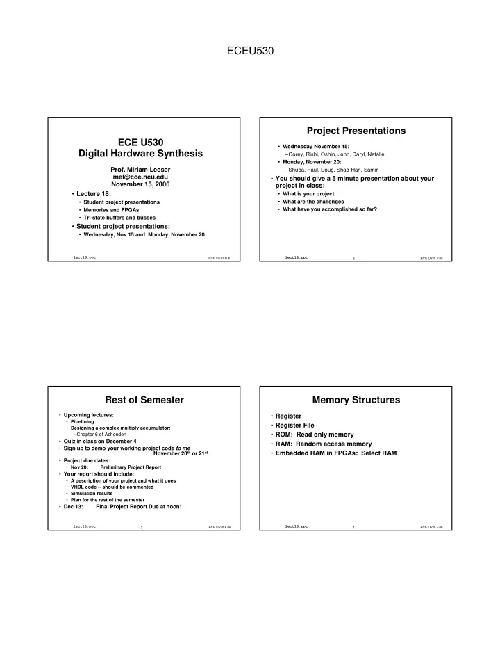
ECEU530 Project Presentations ECE U530 • Wednesday November 15: Digital Hardware Synthesis –Corey, Rishi, Oshin, John, Daryl, Natalie • Monday, November 20: Prof. Miriam Leeser –Shuba, Paul, Doug, Shao-Han, Samir mel@coe.neu.edu • You should give a 5 minute presentation about your November 15, 2006 project in class: • Lecture 18: • What is your project • What are the challenges • Student project presentations • Memories and FPGAs • What have you accomplished so far? • Tri-state buffers and busses • Student project presentations: • Wednesday, Nov 15 and Monday, November 20 lect18.ppt ECE U530 F06 lect18.ppt 2 ECE U530 F’06 Rest of Semester Memory Structures • Upcoming lectures: • Register • Pipelining • Register File • Designing a complex multiply accumulator: • ROM: Read only memory – Chapter 6 of Ashenden • Quiz in class on December 4 • RAM: Random access memory • Sign up to demo your working project code to me November 20 th or 21 st • Embedded RAM in FPGAs: Select RAM • Project due dates: • Nov 20: Preliminary Project Report • Your report should include: • A description of your project and what it does • VHDL code -- should be commented • Simulation results • Plan for the rest of the semester • Dec 13: Final Project Report Due at noon! lect18.ppt lect18.ppt 3 ECE U530 F’06 4 ECE U530 F’06
ECEU530 Basic Memory Operations Memory Block Diagram • A basic memory system is shown Read Memory � Read a data value stored in memory: • m Data Input Lines here: • Place a valid address on the address lines • k address lines are decoded to m • Wait for the read data to become stable address 2 k words of memory Write Memory � Write a data value to memory: • Memory • Each word is m bits k Address Lines Unit k • Place a valid address on the address lines and valid data on • Read and Write are single bit 2 k Words the data lines control lines defining the simple m Bits per 1 • Toggle the memory write control line memory operations Read Word • Sometimes the read or write enable line is defined as a 1 clock with precise timing information (e.g. Read Clock, Write Write Strobe). • Otherwise, it is just an interface signal m • Sometimes memory must acknowledge that it has completed the operation -- handshaking m Data Output Lines lect18.ppt lect18.ppt 5 ECE U530 F’06 6 ECE U530 F’06 Generic RAM (1) Generic RAM (2) ARCHITECTURE behavioral OF ram IS LIBRARY ieee; USE ieee.std_logic_1164.all; TYPE vector_array IS ARRAY (0 TO words-1) OF ---------------------------------------------------------------------- STD_LOGIC_VECTOR(bits – 1 DOWNTO 0); --------------------------- SIGNAL memory: vector_array; ENTITY ram IS BEGIN GENERIC (bits: INTEGER := 8; -- # of bits per word PROCESS(clk, wr_ena) words: INTEGER := 16); -- # of words in the memory BEGIN IF(wr_ena=‘1’) THEN PORT ( wr_ena, clk: IN STD_LOGIC; IF (clk’EVENT AND clk=‘1’) THEN addr: IN INTEGER RANGE 0 to words – 1; memory(addr) <= data_in; data_in: IN STD_LOGIC_VECTOR(bits – 1 downto 0); END_IF; data_out: OUT STD_LOGIC_VECTOR(bits – 1 downto 0) END IF; ); END PROCESS; END ram; data_out <= memory(addr); END ram; lect18.ppt lect18.ppt 7 ECE U530 F’06 8 ECE U530 F’06
ECEU530 Microprocessor Register File Multi-ported Memory • For read operations, • Motivation: functionally the regfile is • Consider CPU core register file: equivalent to a 2-D array of – 1 read or write per cycle limits processor performance. flip-flops with tristate outputs – Complicates pipelining. Difficult for different instructions to on each simultaneously read or write regfile. • MUX, but distributed – Common arrangement in pipelined CPUs is 2 read ports and • Unary control 1 write port – 2 read ports: dual ported memory • Cell with added write logic: These circuits are just functional abstractions of data a the actual circuits used. sel a Regfile sel b sel c data b data c lect18.ppt lect18.ppt 9 ECE U530 F’06 10 ECE U530 F’06 Behavioral Description of a Register Behavioral Description of a Register File File, asynchronous Register File write_cntrl architecture process_behavior of regfile is type reg_array is array(0 to 31) of std_logic_vector (31 downto 0); src1_addr src1_data begin src2_addr 32 regfile_process: process(src1_addr,src2_addr,dst_addr,write_cntrl) words variable data_array: reg_array := ( dst_addr (X”00000000”), src2_data write_data (X”00000000”), . . . 32 bits (X”00000000”)); library IEEE; variable addrofsrc1, addrofsrc2, addrofdst: integer; use IEEE.std_logic_1164.all; begin use IEEE.std_logic_arith.all; addrofsrc1 := conv_integer(src1_addr); addrofsrc2 := conv_integer(src2_addr); entity regfile is addrofdst := conv_integer(dst_addr); port(write_data: in std_logic_vector(31 downto 0); if write_cntrl = ‘1’ then dst_addr,src1_addr,src2_addr: in UNSIGNED(4 downto 0); data_array(addrofdst) := write_data; write_cntrl: in std_logic; end if; src1_data,src2_data: out std_logic_vector(31 downto 0)); src1_data <= data_array(addrofsrc1) after 10 ns; end regfile; src2_data <= data_array(addrofsrc2) after 10 ns; end process regfile_process; end process_behavior; lect18.ppt lect18.ppt 11 ECE U530 F’06 12 ECE U530 F’06
ECEU530 Xilinx FPGA Architecture Using SRAM to Implement Logic ��� ��� ��� ��� ��� ��� ��� ��� ��� ��� CLB Configurable Logic Block IOB Input/Output Block PSM Programmable Switch Matrix PIP Programmable Interconnect Point lect18.ppt lect18.ppt 13 ECE U530 F’06 14 ECE U530 F’06 A Simplified Logic Slice Mapping a Function to a 4-input LUT lect18.ppt lect18.ppt 15 ECE U530 F’06 16 ECE U530 F’06
ECEU530 CLB Used as RAM Memory Blocks in FPGAs • LUTs can double as small RAM blocks: • 4-LUT is really a 16x1 memory. Normally we think of the contents being written from the configuration bit stream, but Virtex architecture (and others) allow bits of LUT to be written and read from the general interconnect structure. • achieves 16x density advantage over using CLB flip-flops. • Furthermore, the two LUTs within a slice can be combined to create a 16 x 2-bit or 32 x 1-bit synchronous RAM, or a 16x1-bit dual-port synchronous RAM. • The Virtex-E LUT can also provide a 16-bit shift register of adjustable length. • Newer FPGA families include larger on- chip RAM blocks (usually dual ported): • Called block selectRAMs in Xilinx Virtex series • 4k bits each lect18.ppt lect18.ppt 17 ECE U530 F’06 18 ECE U530 F’06 Distributed RAM Spartan-IIE Memory Hierarchy RAM16X1S High-Performance External Shift Register LUT Distributed RAM Block RAMs D WE Memory Interfaces • 16 registers, 1 LUT • Single-port • 4Kbit blocks = WCLK O LUT A0 •DDR I/O • CLB LUT configurable as Distributed • Compact & fast • Dual port • True dual-port A1 A2 RAM • Cascadable •SSTL, HSTL, CTT A3 SRL16 Q D D • A LUT equals 16x1 RAM CL SRL16E RAM32X1S Q C K A0 4Kx1 D CL E A1 Port B • Implements Single and Dual-Ports Port A SDRAM WE K A0 2Kx2 A2 WCLK 16x1 A1 A3 1Kx4 SGRAM • Cascade LUTs to increase RAM size A0 O A1 A2 512x8 A2 PB SRAM A3 • Synchronous write A3 256x16 DDR SRAM A4 � Pipelining • Synchronous/Asynchronous read Block RAM ZBT SRAM LUT or RAM16X2S � DSP Coefficients � Buffers D0 • Accompanying flip-flops used for � Small FIFOs QDR SRAM D1 � Cache Tag memory WE synchronous read � Scratch Pad = � Large FIFOs WCLK O0 RAM16X1D A0 O1 � Packet buffers A1 D � Collaboration with A2 WE A3 � Video line buffers WCLK memory vendors Bytes or A0 SPO � IDT, Cypress, LUT A1 Kilobytes A2 Micron, NEC, A3 Samsung, Toshiba... DPRA0 DPO DPRA1 DPRA2 Megabytes DPRA3 lect18.ppt lect18.ppt 19 ECE U530 F’06 20 ECE U530 F’06
ECEU530 FPGA Embedded Memory Summary Memories in VHDL for Xilinx • Look at the Language Templates in Project Manager • Fast distributed RAM for how to describe memories in VHDL for FPGAs • Data right beside logic • Memory requirements solved by Block RAM • Synthesis Templates: • Single and True Dual-Port RAM implementations • Distributed RAM • FIFO for buffering data • Block RAM • Data width conversion • Cache • Register stacks • Component Instantiations • CAM for high-speed parallel searches • Many more • Direct connection to external high-speed memory lect18.ppt lect18.ppt 21 ECE U530 F’06 22 ECE U530 F’06 Tri-State Buffers Using tri-state buffers • The input signal is only connected to the output signal when the Tri-state buffers are like a distributed mux E In Out enable signal is asserted • Tri state buffers are used when multiple gates may need to drive 0 0 Z a single logical signal line 0 1 Z E0 • Care must be taken to ensure that only one output is enabled to 1 0 0 drive the output signal at any given time 1 1 1 I0 E In Out 0 0 Z OUT E1 0 1 Z ENABLE 1 0 0 1 1 1 I1 IN OUT E2 I2 lect18.ppt lect18.ppt 23 ECE U530 F’06 24 ECE U530 F’06
ECEU530 Registers Connected by a Tri-state Bus • Can make any register transfer R[i] ← ← R[j] ← ← • Can’t have G i = G j = 1 for i � j • Violating this constraint gives low resistance path from power supply to ground lect18.ppt 25 ECE U530 F’06
Recommend
More recommend
Explore More Topics
Stay informed with curated content and fresh updates.
