ECEU530 Schedule ECE U530 Homework 6 due Wednesday, November 15 - PDF document
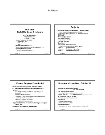
ECEU530 Schedule ECE U530 Homework 6 due Wednesday, November 15 Digital Hardware Synthesis Complete the Calculator from ECEU323 in VHDL Write a controller Prof. Miriam Leeser Combine controller and datapath mel@coe.neu.edu
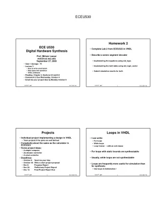
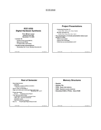
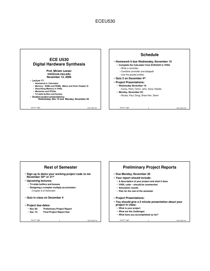
ECEU530 Schedule ECE U530 • Homework 6 due Wednesday, November 15 Digital Hardware Synthesis • Complete the Calculator from ECEU323 in VHDL –Write a controller Prof. Miriam Leeser –Combine controller and datapath mel@coe.neu.edu –Use the posted entities November 13, 2006 • Quiz 2 on December 4 th • Lecture 17: • Project Presentations: • Homework 6: Calculator • Wednesday November 15: • Memory: RAMs and ROMs (Mano and Kime Chapter 9) • Describing Memory in VHDL –Corey, Rishi, Oshin, John, Daryl, Natalie • Memories and FPGAs • Monday, November 20: • Tri-state buffers and busses –Shuba, Paul, Doug, Shao-Han, Samir • Student project presentations: Wednesday, Nov 15 and Monday, November 20 lect17.ppt ECE U530 F06 lect17.ppt 2 ECE U530 F’06 Rest of Semester Preliminary Project Reports • Sign up to demo your working project code to me • Due Monday, November 20 November 20 th or 21 st • Your report should include: • Upcoming lectures: • A description of your project and what it does • Tri-state buffers and busses • VHDL code -- should be commented • Designing a complex multiply accumulator: • Simulation results –Chapter 6 of Ashenden • Plan for the rest of the semester • Quiz in class on December 4 • Project Presentations: • You should give a 5 minute presentation about your project in class: • Project due dates: • What is your project • Nov 20: Preliminary Project Report • What are the challenges • Dec 13: Final Project Report Due • What have you accomplished so far? lect17.ppt lect17.ppt 3 ECE U530 F’06 4 ECE U530 F’06
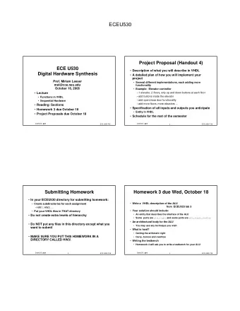
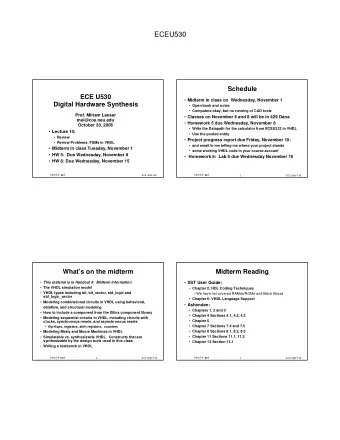
ECEU530 Calculator: Lab 5 Calculator Entity library IEEE; use IEEE.std_logic_1164.all; entity Calc is port (sw: in STD_LOGIC_VECTOR(7 downto 0); -- instruction and data input bus reset: in STD_LOGIC; -- active high reset signal exc: in STD_LOGIC; -- execution signal, active high clk: in STD_LOGIC; -- clock signal dout: out STD_LOGIC_VECTOR (3 downto 0); -- data output cout: out STD_LOGIC -- 4th bit from tos, -- indicates error flag ); end Calc; lect17.ppt lect17.ppt 5 ECE U530 F’06 6 ECE U530 F’06 Calculator Architecture Controller Entity architecture Calc_arch of Calc is component ctrl library IEEE; port (reset: in STD_LOGIC; -- active high reset signal use IEEE.std_logic_1164.all; clk : in STD_LOGIC; -- clock signal entity ctrl is exc : in STD_LOGIC; -- execution signal active high port ( sw : in STD_LOGIC_VECTOR(7 downto 4); -- instruction reset: in STD_LOGIC; -- active high reset signal sm : out STD_LOGIC; -- mux select signal clk : in STD_LOGIC; -- clock signal sa : out std_logic_vector (2 downto 0); -- alu select exc : in STD_LOGIC; -- execution signal, active high ss : out std_logic_vector (1 downto 0)); -- stack select sw : in STD_LOGIC_VECTOR (7 downto 4); end component; -- instruction input component datapath sm: out STD_LOGIC; -- mux select signal port (reset : in STD_LOGIC; -- asynchronous reset sa: out std_logic_vector (2 downto 0); -- alu select din : in std_logic_vector (3 downto 0); -- input data ss: out std_logic_vector (1 downto 0) ); -- stack select dout: out std_logic_vector (3 downto 0); -- output data ); cout : out std_logic; -- carry, borrow or overlow flag end ctrl; sm : in std_logic; -- mux selector architecture ctrl_arch of ctrl is sa : in std_logic_vector (2 downto 0); -- alu select ss : in std_logic_vector (1 downto 0); -- stack select begin clk : in std_logic ); -- clock -- <<enter your statements here>> end component; end ctrl_arch; begin -- <<enter your statements here>> end Calc_arch; lect17.ppt lect17.ppt 7 ECE U530 F’06 8 ECE U530 F’06
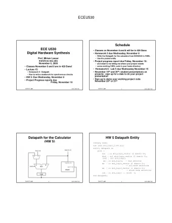
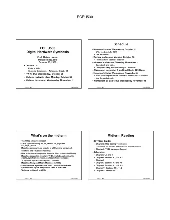
ECEU530 Controller for Calculator Controller for Calculator • Push instruction • Always go through all the states • TOS1: hold stack • TOS2: hold stack, put input in temp register • PUSH: push input • Pop instruction EXE = 0 • TOS1: pop EXE = 1 • TOS2: hold stack Reset Wait TOS1 TOS2 PUSH • TOS3: hold stack • Add TOS1 + TOS2 • TOS1: Put TOS in temp register, pop stack • TOS2: Add TOS to temp register, pop stack • PUSH: Push result lect17.ppt lect17.ppt 9 ECE U530 F’06 10 ECE U530 F’06 Controller State Machine Memory Structures • 3 processes: • Register • state register • Register File • Next state function • ROM: Read only memory • Output function • RAM: Random access memory –What are the outputs • Embedded RAM in FPGAs: Select RAM –Are they Mealy or Moore? »Does it matter? lect17.ppt lect17.ppt 11 ECE U530 F’06 12 ECE U530 F’06
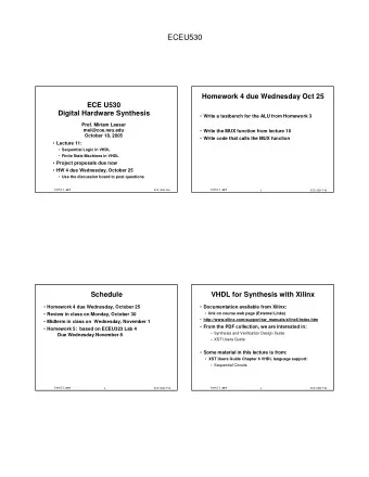
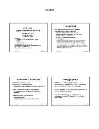
ECEU530 Register (Eight-bit) n-bit Register with Reset D(7) Q(7) entity EXAMPLE is D(6) Q(6) D (7 downto 0) Q(7 downto 0) D(5) Q(5) generic (width : positive := 8); D(4) Q(4) port ( DI : in STD_LOGIC_VECTOR ( width-1 downto 0); D(3) Q(3) CLK : in STD_LOGIC; D(2) Q(2) RST : in STD_LOGIC; Clk D(1) Q(1) DO : out STD_LOGIC_VECTOR (width-1 downto 0) ); end EXAMPLE; D(0) Q(0) architecture ARCHI of EXAMPLE is begin process (CLK, RST) begin Clk if RST = '1' then process(Clk) DO <= (others => ‘0’); begin elsif CLK'EVENT and CLK = '1' then DO <= DI ; if rising_edge(Clk) then end if; Q <= D; end process; end ARCHI; end if; end process; This register has no reset lect17.ppt lect17.ppt 13 ECE U530 F’06 14 ECE U530 F’06 Simplest Memory: Array stored in FFs Stack is an Array stored in FFs • The simplest memory is an array stored in flip-flops • Declaration of STACK: ARCHITECTURE behavioral OF stack IS ______ Flip-flops are inferred SUBTYPE four_bit IS std_logic_vector (3 downto 0); TYPE four_array IS ARRAY (3 downto 0) OF four_bit; SIGNAL stk, tmp : four_array; • Different values can be stored in different locations of begin the stack at different times ... process (reset,clk) • Only top of stack is visible begin if reset = '1' then stk <= (OTHERS => "0000"); • Difference between a stack and more general elsif clk'event and clk = '1' then memory: stack requires no address stk <= tmp; end if; end process; end architecture; lect17.ppt lect17.ppt 15 ECE U530 F’06 16 ECE U530 F’06
ECEU530 Memories RAMs and ROMs • Organized as an indexed array of words. • A ROM with n address input lines and m data output lines contains 2^n entries, each m bits wide • Value of the index for each word is the memory address. • The ROM is said to have a height of 2^n and a width of m • Memory Operations � • read and write operations over some data element: Address –bit, byte, word, etc. A0 Data • Random Access Memory (RAM): A1 D0 • can address any location in memory and read data A2 D1 Inputs A3 • can address any location in memory and write data Outputs D2 A4 • Read Only Memory (ROM): D3 A5 • can address any location in memory and read data A6 • Data is preloaded into memory: no need to write it A7 lect17.ppt lect17.ppt 17 ECE U530 F’06 18 ECE U530 F’06 Generic ROM (1) Filling in a ROM • ROM can be programmed to store arbitrary truth LIBRARY ieee; tables USE ieee.std_logic_1164.all; • Programming a ROM to implement a decoder ------------------------------------------------------------------------------------------------- operation: ENTITY rom IS GENERIC (bits: INTEGER:=8; -- # of bits per word words: INTEGER := 8); -- # of words in the memory Address Contents PORT ( addr: IN INTEGER RANGE 0 to words-1; A B C O7 O6 O5 O4 O3 O2 O1 O0 data: OUT STD_LOGIC_VECTOR(bits – 1 downto 0) 0 0 0 0 0 0 0 0 0 0 1 ); 0 0 1 0 0 0 0 0 0 1 0 END rom; 0 1 0 0 0 0 0 0 1 0 0 0 1 1 0 0 0 0 1 0 0 0 1 0 0 0 0 0 1 0 0 0 0 1 0 1 0 0 1 0 0 0 0 0 1 1 0 0 1 0 0 0 0 0 0 1 1 1 1 0 0 0 0 0 0 0 lect17.ppt lect17.ppt 19 ECE U530 F’06 20 ECE U530 F’06
Recommend
More recommend
Explore More Topics
Stay informed with curated content and fresh updates.
