Slides for Lecture 32 ENEL 353: Digital Circuits Fall 2013 Term - PowerPoint PPT Presentation
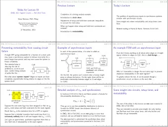
Slides for Lecture 32 ENEL 353: Digital Circuits Fall 2013 Term Steve Norman, PhD, PEng Electrical & Computer Engineering Schulich School of Engineering University of Calgary 25 November, 2013 slide 2/19 ENEL 353 F13 Section 02
Slides for Lecture 32 ENEL 353: Digital Circuits — Fall 2013 Term Steve Norman, PhD, PEng Electrical & Computer Engineering Schulich School of Engineering University of Calgary 25 November, 2013
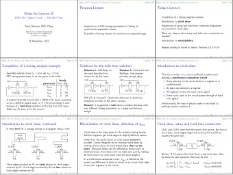
slide 2/19 ENEL 353 F13 Section 02 Slides for Lecture 32 Previous Lecture Implications of DFF timing parameters for timing of synchronous sequential circuits. Examples of timing analysis for synchronous sequential logic.
slide 3/19 ENEL 353 F13 Section 02 Slides for Lecture 32 Today’s Lecture Completion of a timing analysis example. Introduction to clock skew . Adjustment of setup and hold time constraint inequalities to account for clock skew. What can happen when setup and hold time constraints are violated? Introduction to metastability . Related reading in Harris & Harris: Sections 3.5.2–3.5.4
slide 4/19 ENEL 353 F13 Section 02 Slides for Lecture 32 Completion of a timing analysis example Available inverters have t cd = 9 ns and t pd = 15 ns. DFF timing parameters, in ns, are given in the table. family CLK parameter Foo Bar t setup 2 20 Y t hold 1 7 t pcq 8 50 FooLogic BarTron t ccq 5 30 A student tests the circuit with a 1 MHz CLK input, expecting to see a 250 kHz square wave on Y. The circuit doesn’t work because of a hold time violation at the BarTron DFF input. What can be done to fix the circuit?
slide 5/19 ENEL 353 F13 Section 02 Slides for Lecture 32 Solutions for the hold time violation Solution 1: Add delay on Solution 2: Switch the two the path from the Foo flip-flops. One inverter output to the Bar input. provides enough delay. CLK CLK Y Y FooLogic BarTron BarTron FooLogic DIY (Do It Yourself): Check that there are no hold-time violations in either of the above circuits. Remark: It is generally a bad idea to combine flip-flops with very different timing parameters in a single synchronous design!
slide 6/19 ENEL 353 F13 Section 02 Slides for Lecture 32 Introduction to clock skew This list is review. It’s a list of sufficient conditions for building a synchronous sequential circuit . . . 1. Every element in the circuit either is a register or is combinational. 2. At least one element is a register. 3. All registers receive the same clock signal. 4. Every cyclic path in the circuit passes through at least one register. Unfortunately, the laws of physics make it very hard to perfectly satisfy condition 3 . . .
slide 7/19 ENEL 353 F13 Section 02 Slides for Lecture 32 Introduction to clock skew , continued It takes time for a voltage change to propagate along a wire. clock source CLK1 CLK2 CLK3 D1 Q1 D2 Q2 D3 Q3 R1 R2 R3 Clock edges received by R1 are early relative to clock edges received by R2. Clock edges received by R3 are late relative to clock edges received by R2.
slide 8/19 ENEL 353 F13 Section 02 Slides for Lecture 32 Minimization of clock skew; definition of t skew Clock skew is the name given to the problem having having different registers get clock edges at slightly different names. Delay from the clock source to clock inputs cannot be avoided. Circuit designers try to minimize clock skew by making all the source-to-input delays very close to the same . (Because delays can be affected by factors such as electrical noise, clock skew can’t be made zero just by making all clock-source-to-clock-input wires the same length.) In a synchronous sequential circuit, t skew is defined as the worst-case difference in times of arrival of an active clock edge at any two registers in the circuit.
slide 9/19 ENEL 353 F13 Section 02 Slides for Lecture 32 Clock skew, setup and hold time constraints CLK1 and CLK2 come from the same clock source, but due to clock skew, clock edges might not arrive at R1 and R2 at exactly the same time. CLK1 CLK2 D1 Q1 D2 Q2 C L R1 R2 Review: If it happens that that there is no clock skew, then we know for safe operation this must be true . . . t pd for C L ≤ T C − ( t pcq + t setup ) ( t setup constraint) t cd for C L ≥ t hold − t ccq ( t hold constraint)
Clock skew and the setup time constraint slide 10/19 CLK1 CLK2 D1 Q1 D2 Q2 C L R1 R2 Suppose CLK2 is early relative to CLK1. For reliable operation, what must be true about the speed of the combinational logic? (The gold rectangle shows the t setup / t hold aperture for R2.) CLK1 t pcq Q1 t pd D2 CLK2 t skew
Clock skew and the hold time constraint slide 11/19 CLK1 CLK2 D1 Q1 D2 Q2 C L R1 R2 Now suppose CLK2 is late relative to CLK1. For reliable operation, what must be true about the speed of the combinational logic? (Again, the gold rectangle shows the t setup / t hold aperture for R2.) CLK1 t ccq Q1 t cd D2 CLK2 t skew
slide 12/19 ENEL 353 F13 Section 02 Slides for Lecture 32 Summary of timing constraints in the presence of clock skew setup time constraint: t pd ≤ T C − ( t pcq + t setup + t skew ) hold time constraint: t cd ≥ t hold + t skew − t ccq Things to note: ◮ If we set t skew = 0, we get the same inequalities we derived in the previous lecture. ◮ Both inequalities say that as t skew increases, the designer’s job gets more difficult. t pd may need to be reduced on some paths, and t cd may need to be increased on other paths.
slide 13/19 ENEL 353 F13 Section 02 Slides for Lecture 32 Review of a simple timing example Here there is a violation of the setup-and-hold-time rules around t 1 . CLK D Q ? ? ? t 0 t 1 What happens to Q after t 1 ? There are multiple possibilities . Let’s look at these multiple possibilities in more detail.
slide 14/19 ENEL 353 F13 Section 02 Slides for Lecture 32 An odd-looking example circuit CLK Connecting one signal to four register inputs will let D Q 3 us make a point about the Q 2 variety of possible responses Q 1 to an aperture time Q 0 violation. The DFFs in the register are very close to identical, but not perfectly so, due to minor manufacturing variations. If the setup and hold time rules are respected, all four Q values will copy D on each rising edge of CLK, with a delay in the range from t ccq to t pcq . What might happen if the setup and hold time rules are violated?
slide 15/19 ENEL 353 F13 Section 02 Slides for Lecture 32 Example responses to a setup time violation Here we assume that Q 3:0 = 0000 before the rising edge of CLK. CLK D Q 3 Q 2 Q 1 Q 0 Let’s make some remarks about these responses.
slide 16/19 ENEL 353 F13 Section 02 Slides for Lecture 32 Metastability in latches and flip-flops In normal operation the Q and Q signals of a latch or flip-flop will sit in one or the other of two stable states: ( Q , Q ) = (0 , 1) or ( Q , Q ) = (1 , 0). Metastability is the name given to a kind of abnormal behaviour in which the voltages of the Q and Q signals both sit approximately halfway between 0 and V DD for some period of time called t res , the resolution time . Once the resolution time has passed, the latch or flip-flop goes to (“resolves” to) one or the other of its stable states. t res is random , differing in length from one instance of metastability to the next.
slide 17/19 ENEL 353 F13 Section 02 Slides for Lecture 32 A mechanical analogy for metastability There are two stable places for the ball: the bottom of valley 0, and the bottom of valley 1. hill valley 0 valley 1 Given a gentle nudge, the ball will move a little, but stay in valley 0. Given a strong push, the ball will roll over the hill and settle in valley 1. What if the ball is given a push that gives it just enough energy to get to the top of the hill and stop?
slide 18/19 ENEL 353 F13 Section 02 Slides for Lecture 32 Why is metastability dangerous? The key problem is this: t res will sometimes be much longer than t pcq . Sometimes t res may be as long as one whole clock period in a synchronous system. Of course, the output signal of a flip-flop or latch is typically an input signal to one or more other circuit elements. A circuit element with a metastable input will probably generate an incorrect output. So metastability in a single DFF could cause an entire synchronous circuit to behave incorrectly, possibly getting the circuit into a state from which it can’t recover.
slide 19/19 ENEL 353 F13 Section 02 Slides for Lecture 32 Upcoming topics More about metastability. The problem of asynchronous inputs to synchronous systems. Counters and shift registers. Memory arrays. Related reading in Harris & Harris: Sections 3.5.4–3.5.5, 5.4, 5.5
Recommend
More recommend
Explore More Topics
Stay informed with curated content and fresh updates.
![MARKDOWN SLIDES [EN] MARKDOWN SLIDES [EN] MARKDOWN SLIDES [EN] MARKDOWN SLIDES [EN] MARKDOWN](https://c.sambuz.com/818511/markdown-slides-en-markdown-slides-en-markdown-slides-en-s.webp)


