Pre-Knowledge - PDF document
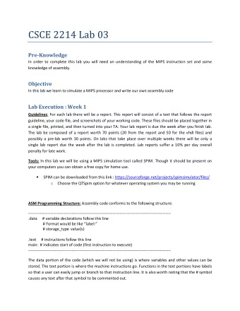
Pre-Knowledge In order to complete this lab you will need and understanding of VHDL as well as patience (an important quality for any computer engineer).
�����������������–���������� Pre-Knowledge In order to complete this lab you will need and understanding of VHDL as well as patience (an important quality for any computer engineer). Objective In this lab we will cover lab guidelines as well as a reviewing vhdl programming paradigms. Additional Materials 1 - VHDL Tutorial Learn by Example : http://esd.cs.ucr.edu/labs/tutorial/ Some VHDL code examples to help you be familiar with the language. 2 – Book: The Designer’s Guide to VDHL by Peter J. Ashenden Lab Execution Guidelines : For each lab there will be a report. This report will consist of a text that follows the report guideline, your vhdl code file, and screenshots of your working code. These files should be placed together in a single file, printed, and then turned into your TA. Your lab report is due the week after you finish lab. The lab be composed of a report worth 70 points (20 from the report and 50 for the vhdl files) and possibly a pre-lab worth 30 points. On labs that take place over multiple weeks there will be only a single lab report due the week after the lab is completed. Lab reports suffer a 10% per day overall penalty for late work. Tools: In this lab we will be using two sets of tools: Xilinx ISE and Modelsim. In the first lab we will only use ISE. To use ISE navigate to the program by following the file path specified. C:\ProgramData\Microsoft\Windows\Start Menu\Programs\Xilinx ISE Design Suite 12.3\ISE • Design Tools\64-bit Project Navigator When you start up ISE you may have a license problem. If you do a dialogue box will open that provides several options for handling licensing problems. Complete the following steps to resolve your licensing issue: In the dialogue box that opens, select the Manage Xilinx Licenses tab • Enter "2011@hthreads.ddns.uark.edu" for XILINXD_LICENSE_FILE and click Set • After the list populates, enter "1717@comp.uark.edu" for LM_LICENSE_FILE and click Set • Click Ok in any dialog boxes •
Click Close • VHDL Programming instructions: For this lab your goal is to create and test a modulo 10 counter. This is simply a counter that counts from 0 to 9. The counter should have a Clock, Enable, and Reset signal. The counter has the following functionality. The clock is positive edge triggered (the circuit changes when the clock goes from 0 to 1) • Enable is active high (the circuit is enabled when the enable signal is a 1) • o When enable is not active the system does not count Reset is active high (the system resets to 0 when the reset signal is a 1) • o Reset is synchronous and happens regardless of the value of enable To create the counter you will need to create a new vhdl project with ISE. In order to do this, follow the guide presented below. 1. Open the ISE 2. Create a new project
3. Chose the location and give a name to your project : Do not use the default user directory. It is write only. Instead select your desktop or documents directory and create a lab folder. 4. Make sure the family is Virtex5 5. Click the next and finish.
6. Add a new VHDL module into your projec: Right click the project, chose New Source 7. Chose VHDL Module and give it a name.Then Click next
8. Click Next and Finish. From this point on you are free to program the counter. If you are unsure of your VHDL skills or need a quick refressher, several tutorial websites have been downloaded and placed in the zip file containing this lab. Creating a test bench: Once you are finished with the counter you will need to test it. A test bench is a file that allows you to determine if a module you have created functions as intended. In vhdl this is a file that contains our counter as a component. The testbench will have a signal for each input and output present on the component. The test bench will write values to the input signals in the component and see what the output looks like. The output will be displayed in waveform format. In this lab we will use ISE to generate a basic testbench template that we will then fill in. To create the testbench, follow the guide presented below. 1. Right click the project, chose New Source
2. Chose VHDL Test Bench and give it a name.Then Click next 3. On the next screen select the source file you wish to create a testbench for (in this case our counter), and click next and then finish.
In your generated testbench you will see several things. The entity statement: an empty entity statement (a testbench does not have input or output signals) The Architecture statement: Declarations 1. A component declaration for the component you are testing. This allows the design to be instantiated in the testbench. 2. Signal declarations designated inputs and outputs. These are internal signals that match up with the signals we wish to test on the component. We will manipulate the inputs and watch the outputs to test our design. 3. A constant declaration called CLK_period. This is how long our clock period will be. The Architecture statement: Component and process statements 1. You will see your component declared a. It will be called uut (Unit Under Test) b. The name will be followed by the component name and a port map statement c. This declaration is similar to declaring an instance of a class in an object oriented programming language. 2. The CLK_process declaration: This process has no sensitivity list so it will continually run over and over again. The process consists of assigning a value of 0 or 1 to the clock followed by a wait of half the defined CLK_period. a. This process is responsible for alternating the clock as the simulation runs 3. The Stimulus process: this process is used to assign values to the circuit inputs. It also has no sensitivity list and as such must always end with a “wait;” statement so that it does not loop forever. In order to test your design you should assign values to your reset and enable signals and see what happens. To do this assign values to those signals you wish to test then use the “wait for # ns;” command (where # is replaced by a numerical value that should be some multiple of CLK_period). This will allow your design to run for that period of time (and thus allow the output of your circuit for those values to appear in the waveform). From that point on you should test all combinations of inputs to verify your circuit works. Example: reset <=1; wait for 100 ns; reset <=0; wait for 100 ns; -- resetting the system sig_1 <= 0; sig_2 <=0; …. sig_N <= 0; wait for 100 ns; -- beginning stimulus testing sig_1 <= 1; sig_2 <=0; …. sig_N <= 0; wait for 100 ns; sig_1 <= 0; sig_2 <=1; …. sig_N <= 0; wait for 100 ns; ... sig_1 <= 1; sig_2 <=1; …. sig_N <= 1; wait for 100 ns; -- end stimulus testing
NOTE: ALWAYS RESET YOUR SYSTEM FIRST IN YOUR STIMULUS PROCESS. Once you’ve finished your test bench you can simulate it from within ISE by clicking on the simulation option in the design viewbox (the one with all the file dropdowns), selecting your testbench, expanding the ISim simulator option below, and clicking simulate behavioral model (Note: you may have to zoom out in the window that opens). You can also click Behavioral Check Syntax to check your code for correct syntax. ----------------------------> Lab Week 2 : As mentioned earlier this is a two week lab. The lab assignment for next week builds upon what we have accomplished this week. Your assignment is to design a clock consisting of modulo 60 counters and a modulo 24 counter. The counters have the same specification as provided above. You should also design a test bench for your clock. Note: your clock does not need to tell time accurately, it only needs to operate functionally. Lab 1 Report Information : The report for this lab should include code and screenshots from both weeks of lab. The text portion of the report should refer to both weeks of lab.
Recommend
More recommend
Explore More Topics
Stay informed with curated content and fresh updates.
