CSCE 2214 Lab 06 Pre-Knowledge In order to complete this lab you - PDF document
CSCE 2214 Lab 06 Pre-Knowledge In order to complete this lab you will need to understand the function of the CPU control block, and the sign extend block Pre-Lab The pre- lab for this week is shown at the end of last weeks lab. Objective In
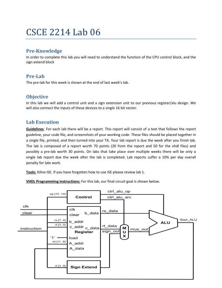
CSCE 2214 Lab 06 Pre-Knowledge In order to complete this lab you will need to understand the function of the CPU control block, and the sign extend block Pre-Lab The pre- lab for this week is shown at the end of last week’s lab. Objective In this lab we will add a control unit and a sign extension unit to our previous register/alu design. We will also connect the inputs of these devices to a single 16 bit vector. Lab Execution Guidelines : For each lab there will be a report. This report will consist of a text that follows the report guideline, your code file, and screenshots of your working code. These files should be placed together in a single file, printed, and then turned into your TA. Your lab report is due the week after you finish lab. The lab is composed of a report worth 70 points (20 from the report and 50 for the vhdl files) and possibly a pre-lab worth 30 points. On labs that take place over multiple weeks there will be only a single lab report due the week after the lab is completed. Lab reports suffer a 10% per day overall penalty for late work. Tools: Xilinx ISE. If you have forgotten how to use ISE please review lab 1. VHDL Programming instructions: For this lab, our final circuit goal is shown below.
Control Unit: In order to design the control unit we must have an understanding of the input into the control and its outputs. The op code value is 4 bits long and the corresponding instruction (to be used in this lab) is given in the table below : Opcode(Binary) Operation 0000 ADD 0001 SUB 0010 AND 0011 OR 0100 ADDI 0101 SUBI As example, if the opcode = 0100, the operation to execute is the immediate addition (ADDI) with the value of the second operand coming from the sign extend unit. Therefore, the signal ctrl_alu_op should be equal to “00” for addition and ctrl_alu_src be set to 1 so that the mux unit will select the incoming signal from the extend unit. The following interface could be used to implement the control block: Entity Control is Port( op : in std_logic_vector(3 downto 0) ; alu_op: out std_logic_vector(1 downto 0) ; alu_src: out std_logic ); End control; Sign Extend: In order for our immediate instructions to work we need to design a sign extend module. This module will take a 4 bit number and extend the number to be 16 bits. If the 4 bit number ends in a 1 then 1’s are extended (to keep the sign negative). If the 4 bit number ends in a 0, then 0’s are extended (to keep the sign positive). An example of a sign extend is shown below.
Your instructions for this portion of the lab are to design a sign extend module that implements the following functionality. Mux Unit: this is simply a 2 to 1 multiplexer, as the one designed in Lab4 (but with less input signals). Assembling Your Design: The final portion of the assignment is to create a single module by combining the control block, the sign extend block, the register file, and the ALU along with adding a multiplexer (which you may implement as well). The design should follow that of the first image in this report. The top-level module has 3 inputs: instruction, clear, and clk. Instruction is a 16 bit input, while clear and clk are 1 bit inputs. Though the module depicted above has no outputs, it is recommended that the Sout_alu signal also connects to some output (otherwise it will be very hard to test using a testbench as you will not be able to see outputs).
Recommend
More recommend
Explore More Topics
Stay informed with curated content and fresh updates.


