Slides for Lecture 20 ENEL 353: Digital Circuits Fall 2013 Term - PowerPoint PPT Presentation
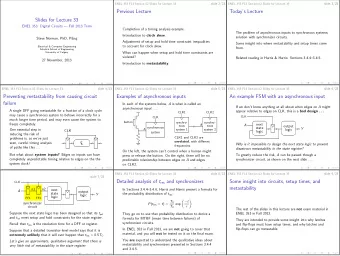
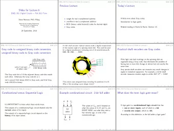
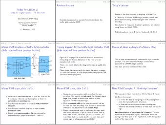
Slides for Lecture 20 ENEL 353: Digital Circuits Fall 2013 Term Steve Norman, PhD, PEng Electrical & Computer Engineering Schulich School of Engineering University of Calgary 25 October, 2013 slide 2/16 ENEL 353 F13 Section 02 Slides
Slides for Lecture 20 ENEL 353: Digital Circuits — Fall 2013 Term Steve Norman, PhD, PEng Electrical & Computer Engineering Schulich School of Engineering University of Calgary 25 October, 2013
slide 2/16 ENEL 353 F13 Section 02 Slides for Lecture 20 Previous Lecture 4:1 multiplexer implementations. Using multiplexers to implement combinational logic functions. Decoders and applications of decoders.
slide 3/16 ENEL 353 F13 Section 02 Slides for Lecture 20 Today’s Lecture Completion of decoder-with-enable examples. (Related reading in Harris & Harris: None.) Introduction to timing of combinational logic; propagation and contamination delays. (Related reading in Harris & Harris: Section 2.9. Careful reading of this section is highly recommended!)
slide 4/16 ENEL 353 F13 Section 02 Slides for Lecture 20 Using small decoders with enable inputs to make bigger decoders Let’s build a 3:8 decoder A 2:4 decoder with enable using an inverter and two input EN . . . 2:4 decoder-with-enable Y 3 circuits. 11 A 1 2:4 Y 2 10 Let’s build a 4:16 decoder- A 0 decoder Y 1 01 with-enable using some 2:4 EN decoder-with-enable Y 0 00 circuits.
slide 5/16 ENEL 353 F13 Section 02 Slides for Lecture 20 Introduction to timing of combinational logic The definition of combinational logic is that the outputs of a combinational element depend only the current values of its inputs. In reality, combinational elements have very, very short “reaction times”. Changes in inputs trigger changes to outputs that are almost but not quite instant . Delays in combinational logic can set important limits on how fast digital systems can operate. We’re about to study some simple methods for estimating overall delays when complex combinational elements are built from simpler combinational elements.
slide 6/16 ENEL 353 F13 Section 02 Slides for Lecture 20 How short is a picosecond? 1 ps = 1 × 10 − 12 s. Every second contains 10 12 = 1 trillion picoseconds. For simple logic gates in today’s integrated circuits, propagation delays—reaction times to changes in input values—are typically tens of picoseconds. An Olympic sprinter is considered to have false-started if she or he has reacted to the starting gun in less than 0.100 seconds. Let’s compare logic gates and humans using the same units for time . . . Typical AND gate reaction time: 60 ps. Very fast human reaction time: 100 , 000 , 000 , 000 ps.
slide 7/16 ENEL 353 F13 Section 02 Slides for Lecture 20 Sketching logic levels as functions of time When a logic signal changes value, voltage as a function of time will follow a curve dictated by some complex physics: V DD voltage 0 time In making sketches to illustrate digital circuit timing, the exact shapes of voltage/time curves are not important, and this style of drawing is often used: 1 logic level 0 time
slide 8/16 ENEL 353 F13 Section 02 Slides for Lecture 20 Delay in a simple gate By convention, delay is A Y measured ◮ from the time that the input is halfway delay between LOW and A HIGH; ◮ to the time that the Y output is halfway between LOW and Time HIGH. Image is Figure 2.66 from Harris D. M. and Harris S. L., Digital Design and Computer Architecture, 2nd ed. , c � 2013, Elsevier, Inc.
slide 9/16 ENEL 353 F13 Section 02 Slides for Lecture 20 A combinational element will exhibit a range of delays There is no single “reaction time” for a given combinational element. Here are some of the many reasons for this: ◮ HIGH-to-LOW output transitions may be faster or slower than LOW-to-HIGH transitions, depending on the design of the element. ◮ Circuits tend to get slower as they get warmer. ◮ Supposedly identical gates may perform differently due to due to variations in manufacturing. ◮ In elements with multiple output bits, some output bits may switch faster than others.
slide 10/16 ENEL 353 F13 Section 02 Slides for Lecture 20 Propagation and contamination delays Because any combinational element exhibits a range of delays, delay characteristics of an element are often described by two numbers : ◮ t pd , the propagation delay . This is the maximum possible delay under the expected operating conditions for the element. ◮ t cd , the contamination delay . This is the minimum possible delay under the expected operating conditions for the element.
slide 11/16 ENEL 353 F13 Section 02 Slides for Lecture 20 t pd and t cd illustrated in a timing diagram A Y This is a relatively simple t pd timing diagram, but there is still a lot going on here! A Let’s make some notes Y about how to read this diagram. t cd Time Image is Figure 2.67 from Harris D. M. and Harris S. L., Digital Design and Computer Architecture, 2nd ed. , c � 2013, Elsevier, Inc.
slide 12/16 ENEL 353 F13 Section 02 Slides for Lecture 20 Example propagation and contamination delays A detailed simulation of a 2-input A Y NAND gate design produces the data B shown in the sketch below . . . 1 A 0 1 B 0 1 Y 0 100ps 130ps 220ps 280ps 350ps 380ps 150ps 200ps What does the data tell us about t pd and t cd for this NAND gate design?
slide 13/16 ENEL 353 F13 Section 02 Slides for Lecture 20 What are the causes of delays? One major cause is the fact that a node in a logic circuit acts as a capacitor . That puts a limit on the rate of change of voltage at a node. I I = C dV dt , so dV dt = I + C . V C − Another important cause is wire delay —it takes a small amount of time for a voltage change to get from one end of a wire to the other, even for the tiny wires within integrated circuits. We won’t study the physical causes of delay in ENEL 353. It’s an important topic in ENCM 467 (Digital Electronics).
slide 14/16 ENEL 353 F13 Section 02 Slides for Lecture 20 Overall t pd and t cd calculations Suppose a combinational system is built by wiring together some combinational elements. C C L L C L C L If we have t pd and t cd data for each of the elements, how can we find overall values of t pd and t cd for the system as a whole ? We’ll see that solving this problem involves concepts called the critical path and the short path .
slide 15/16 ENEL 353 F13 Section 02 Slides for Lecture 20 A simple example of t pd and t cd calculations gate t pd t cd A AND 50 35 B OR 60 45 C Y (Times given D in ps.) What is the critical path for this circuit? What is the short path? What is the overall t pd ? What is the overall t cd ?
slide 16/16 ENEL 353 F13 Section 02 Slides for Lecture 20 Upcoming topics Completion of material on critical paths and short paths, and more examples. Glitches. Related reading in Harris & Harris: Section 2.9.
Recommend
More recommend
Explore More Topics
Stay informed with curated content and fresh updates.
![MARKDOWN SLIDES [EN] MARKDOWN SLIDES [EN] MARKDOWN SLIDES [EN] MARKDOWN SLIDES [EN] MARKDOWN](https://c.sambuz.com/818511/markdown-slides-en-markdown-slides-en-markdown-slides-en-s.webp)


