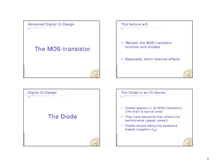

Advanced Digital IC-Design This lecture will Refresh the MOS-transistor function and models The MOS-transistor Especially short channel effects Especially, short channel effects Digital IC-Design The Diode in an IC-device Diodes appears in all MOS-transistors Diodes appears in all MOS-transistors (the drain & source area) The Diode They have parasitics that affects the performance (speed, power) Diodes should always be backward y biased (negative V BS ) 1
Diode - The Simplest IC-device Advanced Digital IC-Design Discrete IC- structure component p SiO 2 The MOS Transistor Metal p + n + p + Semi- n + conductor p - pn -junctions The MOS-transistor: An Old Invention What is a MOS-transistor? MOS = ”Metal Oxide Semiconductor” In 1925, Julius Edgar Lilienfeld described the first MOSFET structure Polysilicon Polysilicon - U.S. Patent in 1930 U S Patent in 1930 SiO 2 In early thirties, a similar structure was shown by Oskar Heil Metal - British Patent in 1935 Silicon, doped Oxide None of them built a working component None of them built a working component Semiconductor The first working MOS-transistor was shown in the early sixties 2
The MOS-transistor (or MOSFET) N-MOS Transistor Gate Most important device in digital design Silicon Bulk Source Drain Structure St t V Very good as a switch d i h Relatively few parasitics p + p + n + n + Each box in the Thin layout represents Rather low power consumption Oxide a mask or a step p - in the process High integration density Simple manufacturing Mask Layout Economical for large complex circuits P-MOS Transistor How does it Work? V GS must be Opens a lager than a Gate Technologies channel Bulk Source Drain threshold V T T N-Well N W ll V DS drives V DS P-Well V GS a current I D n + p + p + p + Twin-Tub n - I D p - N-Well The gate length The gate length Gate Gate sets the name of Source Drain the technology 3
What is a MOS Transistor? MOS – a Four Terminal Device Gate voltage controls the current from drain to source Source connected to lower potential for n -channel devices A Switch Circuit Symbol (often to GND ) ( ) Source connected to higher potential for p -channel devices (often to V DD ) V GS V GS G G Bulk keeps the substrate at a stable potential. If not shown R on eq – it is assumed to be connected to the supply/ GND. S D S D Gate Gate Source Source Drain Drain Infinite resistance when V GS < V T Source Drain Bulk (Body) R eq when V GS ≥ V T V T = Threshold voltage Bulk (Body) Important Dimensions How does the Transistor Work? Technology When V GS is slightly increased development: Gate Negative charges are attracted g g Drain Source Source 1993: 0.6 um W A depletion region is formed 2003: 65 nm t ox 2013: 18 nm? V GS > 0 L L n + n + Depletion The technology is “Diode area” p - Region named after the gate length L 4
How does it Work? Linear Region (Resistive Operation) When V GS is increased above V T V DS is increased slightly More negative than positive charges are attracted Horizontal E-field from drain to source close to the gate (turns to n -type material) A current I D is established A channel is formed (Strong inversion) V GS > V T V GS > V T V DS <V GS -V T I D I D n + n + n + n + n -channel n -channel Depletion Depletion Region Region p - p - Linear Region (Resistive Operation) Linear Region (Resistive Operation) I D is proportional to the vertical E-field = μ ξ μ = I Q W Electron mobility D n n ξ = � i.e. to the # of charges attracted by the gate voltage V GS E-field over the c hannel I D is proportional to the horizontal E-field − ∼ Q V V # of charges attracted by the gate � i.e. to the charge velocity caused by the drain voltage V DS GS T ∼ Q V Less char ges in drain region DS W V = − − DS I k ´ ( V V ) V V V GS forms a ξ = D n GS T DS DS L 2 L vertical E-field n + I D I W V = = μ DS I k ´ ( V - V - ) V ( k ' C ) n + � � � � � � � D n GS T D S n n ox L 2 V DS establish a From Horizontal E-Field horizontal E-field p - From charge conc. 5
Saturation Region Saturation Region V DS = V GS – V T Insert V DS = V GS - V T in the linear equation Strong inversion reached precisely (i.e. V GD = V T ) No channel close to the drain W V = − − DS I k ´ ( V V ) V V GS > V T D n GS T DS L 2 V DS =V GS -V T − I D W V V = − − − GS T I k ´ ( ( V V )( )( V V ) ) D D D n n GS GS T T GS GS T T L 2 n + n + k ´ W = − 2 ”V DS /2" n I ( V V ) D GS T 2 L p - Channel Length Modulation Channel Length Modulation ⇒ V DS > V GS -V T Pinch off Saturation The effective channel length is modulated by V DS g y DS V DS > V GS -V T Electrons are injected through the depletion region V GS >V T W V DS >V GS -V T = − + λ 2 I k ´ ( V V ) (1 V ) D n GS T DS L I D D Pinch off n + n + λ = Empirical constant L´ L 6
The Threshold Voltage V T The Bulk (Body) Potential The substrate is slightly doped (p - for NMOS) The bulk is most often connected to GND ( V DD for PMOS) Negative V SB opens the diode; Not Allowed There are always free electrons in the substrate Positive V SB makes it harder to attract negative charges to V To form a channel, we need to attract these negative charges T f h l d t tt t th ti h P iti k it h d t tt t ti h t the channel The threshold is when the number of negative and positive charges are equal That is, the threshold voltage will increase The value of V T is thus set by the p -doping concentration V GS V SB V GS > V T p + n + n + n + n + Strongly p-doped n -channel Depletion p - Region p - The Threshold Voltage V T MOS Model for Long Channels = + γ − φ + − − φ Widely used model for manual calculations V V ( 2 V 2 ) T T 0 F SB F 2 W V ≤ − = − − + λ DS V V V ; I k ´ (( V V ) V )( 1 V ) φ F = Fermi potential DS GS T D n GS T DS DS L 2 k ´ W γ increases with the acceptor concentration ≥ − = − + λ 2 n V V V ; I ( V V ) ( 1 V ) DS GS T D GS T DS 2 L Low threshold ⇒ Low voltage transistors but Added to avoid discontinuity y they are leaky y y = μ μ k k ´ C C n n ox Two threshold voltage technologies can be used for low power = + γ − φ + − − φ V V ( 2 V 2 ) T T 0 F F SB 7
Velocity & Mobility Velocity & Mobility μ μ The electron (hole) velocity is related to the mobility ( ) ( ) The electron (hole) velocity is related to the mobility ξ ξ The velocity is also dependent on the E-field ( ) ( ) The velocity is also dependent on the E-field 2 m μ = 0.038 = Electron mobility Typical n Vs m 0.35 μ m υ = μ ξ 2 m μ = technology n n 0.013 = Hole mobility s p Vs m m υ = μ ξ The mobility is dependent on doping concentration … p p s Often determined empirically Note that the electron mobility is about 3 times higher υ υ ( ) ( ) Velocity Saturation Velocity Saturation sat sat ξ υ = μ ξ ( ) V DS forms a horizontal E-field E An increased E-field leads to higher electron velocity n n DS ξ ξ ( ( ) ) However at a critical E-field , the velocity saturates due However at a critical E field the velocity saturates due c ν to collisions with other atoms n (m/s) Constant Velocity 5 m nt Mobility υ ≈ ν 10 for both electrons and holes The mobility is sat sat = 10 5 m/ s s not constant when velocity Constan saturation is ξ Source Drain reached n + n + E DS [V/ u m] V DS establish a horizontal E-field ξ 0 E sat p - c 8
I D versus V DS I D versus V GS I D (mA) 0.5 -4 6x 10 -4 2.5x 10 V GS -V T = 2.5 - 0.43 = 2.07 V Long channel Long-channel 5 0.4 model 2 linear 4 quadratic 1.5 V GS = V DD = 2.5 0.3 I D (A) I D (A) 3 Short-channel 1 For both 2 0.2 model 0.5 1 quadratic d ti V DSAT = 0.63 V 0.1 0 0 0 0.5 1 1.5 2 2.5 0 0.5 1 1.5 2 2.5 V GS (V) V GS (V) V DS (V) Long Channel Short Channel 0 0 0.5 1.0 1.5 2.0 2.5 I D versus V DS Model for Manual Analysis Linear I D (V GS ) Quadratic I D (V GS ) V DS = V GS - V T A first order model of the velocity 0 6 0.6 0.25 0 25 V GS = 2.5 I D (mA) I D (mA) 0.5 V GS = 2.5 0.2 υ = μ ξ ξ ≤ ξ ⎧ V GS = 2.0 for 0.4 V GS = 2.0 0.15 n c ⎪ 0.3 ⎨ V GS = 1.5 0.1 V GS = 1.5 0.2 ⎪ ⎪ υ = υ = μ ξ ξ ξ ξ ≥ ≥ ξ ξ V GS = 1.0 0 05 0.05 GS ⎩ ⎩ for f 0.1 V GS = 1.0 sat n c c 0 0 0 0.5 1 1.5 2 2.5 0 0.5 1 1.5 2 2.5 V DS (V) V DS (V) Long Channel Short Channel 9
Recommend
More recommend