Spin field effect transistor 2018.12.21 - PowerPoint PPT Presentation
Spin field effect transistor 2018.12.21 Background Moores law : The number of transistors in a dense integrated circuit doubles about every two years
Spin field effect transistor 2018.12.21 主讲人:张仕雄 组员:杨洁、朱鹏飞、赵嘉佶、梁栋、丁石磊
Background • Moore’s law : The number of transistors in a dense integrated circuit doubles about every two years https://en.wikipedia.org/wiki/Moore%27s_lawv
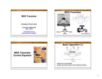
MOSFET • Challenge for MOSFET Heat dissipation problems Quantum tunneling • One of solutions :spin field effect transistor
Rashba SOC in 2DEG • Rashba spin orbit coupling(structure inversion asymetry): • Spin split energy band:
Electro-optic modulator • Different spin polarized electrons have different wave vector • A differential phase shift Datta and Dass.APL.1990
Why choose spin FET? high speed • Property low power consumption high level integration III-V semiconductor Graphene Long spin diffusion length Curie temperature above RT Weak spin orbit coupling Long spin relaxation time Strong spin orbit coupling
How to work? • Spin injection • Spin modulation • Spin detection
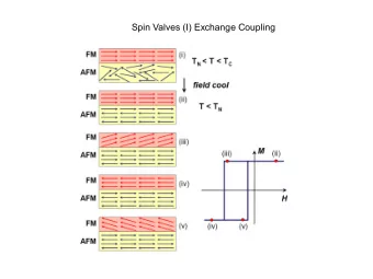
Spin injection • Spin dynamic pumping • Electrical injection Schottky barrier Oxide tunneling barrier Spin Esaki diode Hot electron spin injection
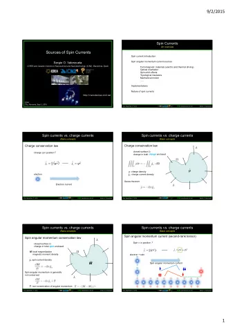
Spin dynamic pumping • Processing magnetization in FM layer pumps spin current into NM layer.
Electrical spin injection theory • Spin polarized current is injected from FM to semiconductor � ↑ �� ↓ • Current spin polarizability � � = � ↑ �� ↓ • Main problem :conductance mismatch • Spin injection efficiency : J.Fabian.et. Review of modern physics.2004
Different contact Spin injection efficiency: • Transparent contact: • Tunneling contact:
Schottky barrier • ferromagnetic Heusler alloy Co 2 FeSi/n-type GaAs S. Sze .et. Metal-semiconductor contacts.2006
Spin Esaki diode Under a small reverse bias electrons from VB of (Ga , Mn)As tunnel to CB of GaAs. The conversion of spin-polarized electrons via Esaki tunneling leaves its mark in a bias dependence of the spin-injection efficiency, which at maximum reaches the value of 50%. ferromagnetic M. Ciorga A.et.prb.2009.
Improvement for depletion region • The use of a thin, heavily doped surface region reduces the depletion width as well as the effective barrier height, significantly enhancing the probability for tunneling.
Oxide barrier • Spin dependent conductance: • Spin efficiency: Zhang.et.PRB.2001
Hot electron spin injection • This method to achieve spin injection is by spin-dependent ballistic hot-electron filtering through ferromagnetic thin films. • The exponential spin selective mean free path dependence in the ferromagnetic films create very large spin polarizations. In principle ,this can approach 1 0 0 % , a l l o w i n g e ff e c t i v e injection and detection at cryogenic and room temperature. Ian Appelbaum.et.nature.2007
Spin detection • ISHE • Silsbee-Johnson spin-charge coupling
AHE,SHE and ISHE • Charge current: • Spin current: • Including spin-orbit coupling and anomalous current density SHE AHE and ISHE
ISHE • Spin current convert to charge current: • Some challenges: Voltage detectable is small(is proportional to the resistivity and ) The device’s dimensions are smaller than
Silsbee-Johnson spin-charge coupling • If a spin accumulation is generated in a nonmagnetic conductor that is in a proximity of a ferromagnet, a current flows in a closed circuit, or an electromotive force appears in an open circuit.
Spin modulation • Hanle spin procession frequency • Spin diffusion length • Conductivity • Spin dependent barrier • Magnetoelectric effect
Spin procession frequency • Spin orbit coupling in 2DEG • Gate modulation of Rashba coefficient • At low temperature,transport of electrons in 2DEG is ballistic(coherent). Hyun Cheol Koo et. science.2009
Spin diffusion length • At RT, in semiconductor(GaAs,GaN),electron spin relaxation dominates by DP mechanism G.Wang.et.nature cm.2013
A spin field-effect switch • Gate voltage modulate the conductivity of MoS2 Wenjing Yan.et.nature cm.2016
Spin-dependent barrier • Using magnetic insulator rather than normal insulator as dielectric layer in FET could induce a spilt according to spin caused by ferromagnetic proximity. PHYSICAL REVIEW B 77, 115406 (2008)
A proposal for spin FET If such structure is deposited on the middle of a non-local spin-valve, the signal would be affected by the gate voltage.
Magnetoelectric effect • A dielectric material moving through an electric field would become magnetized. A material where such a coupling is intrinsically present is called a magnetoelectric .
Thank you
Recommend
More recommend
Explore More Topics
Stay informed with curated content and fresh updates.





![Transistor Channel Model [Farquhar and Hasler, 2004] Transistor HH Channel Model [Farquhar and](https://c.sambuz.com/897541/transistor-channel-model-s.webp)
