CS/EE 6710 MOS Transistor Models Electrical Effects Propagation - PDF document
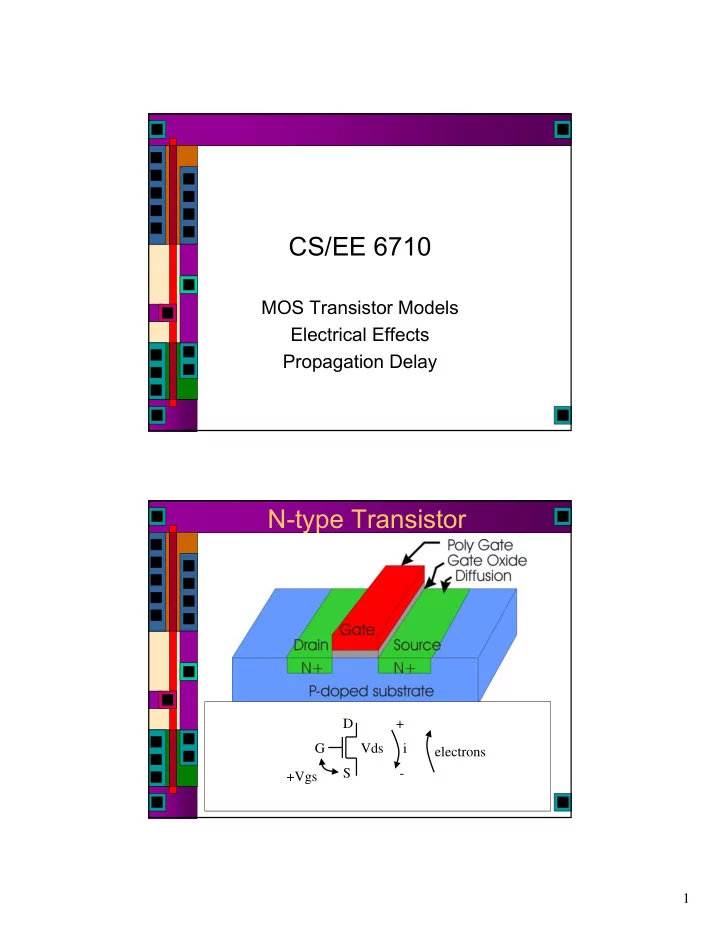
CS/EE 6710 MOS Transistor Models Electrical Effects Propagation Delay N-type Transistor D + G Vds i electrons S - +Vgs 1 Another Cutaway View Thanks to National Central University for Some images Vgs Forms a Channel 2 MOS
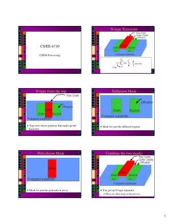
CS/EE 6710 MOS Transistor Models Electrical Effects Propagation Delay N-type Transistor D + G Vds i electrons S - +Vgs 1
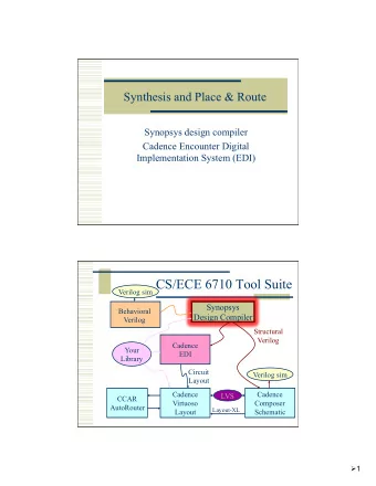
Another Cutaway View Thanks to National Central University for Some images Vgs Forms a Channel 2
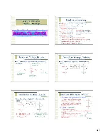
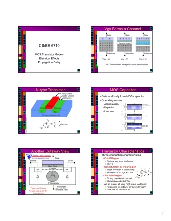
MOS Capacitor � Gate and body form MOS capacitor � Operating modes � Accumulation polysilicon gate V g < 0 silicon dioxide insulator � Depletion + p-type body - � Inversion (a) 0 < V g < V t depletion region + - (b) V g > V t inversion region + depletion region - (c) Transistor Characteristics � Three conduction characteristics � Cutoff Region � No inversion layer in channel � Ids = 0 � Nonsaturated, or linear region D + � Weak inversion of the channel � Ids depends on Vgs and Vds G Vds Ids � Saturated region +Vgs S - � Strong inversion of channel � Ids is independent of Vds � As an aside, at very high drain voltages: � “avalanche breakdown” or “punch through” � Gate has no control of Ids… 3
nMOS Cutoff: Vgs<Vt � No channel � I ds = 0 V gs = 0 V gd + g + - - s d n+ n+ p-type body b nMOS Linear: Vgs>Vt, small Vds � Channel forms � Current flows V gs > V t V gd = V gs + g + from d to s - - s d � e - from s to d V ds = 0 n+ n+ p-type body � I ds increases with b V ds V gs > V t V gs > V gd > V t + g + - - d I ds � Similar to linear s n+ n+ 0 < V ds < V gs -V t resistor p-type body b 4
nMOS Saturation: Vds>Vgs-Vt � Channel pinches off � Conduction by drift because of positive drain voltage � Electrons are injected into depletion region � I ds independent of V ds � We say that the current saturates � Similar to current source V gs > V t V gd < V t g + + - - d I ds s n+ n+ V ds > V gs -V t p-type body b Basic N-Type MOS Transistor � Conditions for the regions of operation � Cutoff: If Vgs < Vt, then Ids is essentially 0 � Vt is the “Threshold Voltage” � Linear: If Vgs>Vt and Vds < (Vgs – Vt) then Ids depends on both Vgs and Vds � Channel becomes deeper as Vgs goes up � Saturated: If Vgs>Vt and Vds > (Vgs – Vt) then Ids is essentially constant (Saturated) D + G Vds Ids electrons S - +Vgs 5
Transistor Gain � β is the MOS transistor gain factor � β = ( με /t ox )(W/L) Layout dependent Process-dependent � μ = mobility of carriers � Note that N-type is twice as good as P-type � ε = permittivity of gate insulator � ε = 3.9 ε 0 for SiO 2 ( ε 0 = 8.85x10 -14 F/cm) � T ox = thickness of gate oxide � Also, ε /t ox =C ox The oxide capacitance � β = ( μ C ox )(W/L) = k’(W/L) = KP(W/L) � Increase W/L to increase gain Example � We will be using a 0.6 μ m process for your project � From AMI Semiconductor � t ox = 100 Å 2.5 V gs = 5 � μ = 350 cm 2 / V*s 2 � V t = 0.7 V 1.5 V gs = 4 I ds (mA) 1 � Plot I ds vs. V ds V gs = 3 0.5 V gs = 2 � V gs = 0, 1, 2, 3, 4, 5 V gs = 1 0 0 1 2 3 4 5 � Use W/L = 4/2 λ V ds ⎛ − ⎞ • ⋅ ⎛ ⎞ 14 W 3.9 8.85 10 W W ( ) β = μ = = μ 2 C 350 ⎜ ⎟ ⎜ ⎟ 120 A V / ⋅ − ox 8 ⎝ ⎠ L ⎝ 100 10 ⎠ L L 6
“Saturated” Transistor � In the 0 < (Vgs – Vt) < Vds case � Ids Current is effectively constant � Channel is “pinched off” and conduction is accomplished by drift of carriers � Voltage across pinched off channel (I.e. Vds) is fixed at Vgs – Vt � This is why you don’t use an N-type to pass 1’s! � High voltage is degraded by Vt � If Vt is 1.0v, 5v in one side, 4.0v out the other 5v 4.0v D S G 5v Aside: N-type Pass Transistors A Out ~S B S � If it weren’t for the threshold drop, N-type pass transistors (without the P-type transmission gate) would be nice � 2-way Mux Example… 7
N-type Pass Transistors 5v 4.0v 0.0v G 5v � One one hand, the degraded high voltage from the pass transistor will be restored by the inverter � On the other hand, the P-device may not turn off completely resulting in extra power being used N-type Pass Transistors 5v 4.0v 0.0v G 5v � Another option is a “keeper” transistor fed back from the output � This pulls the internal node high when the output is 0 � But is disconnected when output is high � Make sure the size is right… 8
N-type Pass Transistors � In practice, they are used fairly often, but be aware of what you’re doing � For example, read/write circuits in a Register File * WE RE0 RE1 D0 D1 Write Data Read Data Back to the Saturated Transistor � What influences the constant Ids in the saturated case? � Channel length � Channel width � Threshold voltage Vt � Thickness of gate oxide � Dielectric constant of gate oxide � Carrier mobility μ � Velocity Saturation 9
Threshold Voltage: Vt � The Vgs voltage at which Ids is essentially 0 � Vt = .67v for nmos and -.92v for pmos in our process � Tiny Ids is exponentially related to Vgs, Vds � Take 5720/6720 for “subthreshold” circuit ideas � Vt is affected by � Gate conductor material � Gate insulator material � Gate insulator thickness � Channel doping � Impurities at Si/insulator interface � Voltage between source and substrate (Vsb) 2 nd Order Effect: Body Effect � A second order effect that raises Vt � Recall that Vt is affected by Vsb (voltage between source and substrate) � Normally this is constant because of common substrate � But, when transistors are in series, Vsb (Vs – Vsubstrate) may be changed Vt2 Vsb2 = 0 Vt2 > Vt1 Vt1 Vsb1 = 0 10
Basic DC Equations for Ids � Cutoff Region D + � Vgs < Vt, Ids = 0 G Vds Ids � Linear Region S - +Vgs � 0 < Vds < (Vgs – Vt) Ids = β [(Vgs – Vt)Vds – Vds 2 /2] � Note that this is only “linear” if Vds 2 /2 is very small, I.e. Vds << Vgs –Vt � Saturated Region � 0 < (Vgs – Vt) < Vds Ids = β [(Vgs – Vt) 2 /2] Ids Curves 11
P-type Transistor S + -Vgs G Vsd i holes - D P-type Transistor 12
P-type Transistors � Source is Vdd instead of GND � Vsg = (Vdd - Vin), Vsd = (Vdd -Vout), Vt is negative -Vgs � Cutoff: (Vdd-Vin) < -Vt, Ids=0 S + Vsd i G � Linear Region - D � (Vdd-Vout) < (Vdd - Vin + Vt) Ids = β [(Vdd-Vin+Vt)(Vdd-Vout) – (Vdd-Vout) 2 /2] � Saturated Region � ((Vdd - Vin) + Vt) < (Vdd - Vout) Ids = β [(Vdd -Vin + Vt) 2 /2] Pass Transistor Ckts V V V DD DD DD V V DD DD V DD V DD V DD V SS 13
Pass Transistor Ckts V V V DD DD DD V V DD DD V V DD -V tn DD V s = V DD -V V DD -V tn V DD -V tn tn V DD V DD -V V s = |V tp | tn V V DD -2V DD tn V SS 2 nd Order Effect: Velocity Saturation � With weak fields, current increases linearly with lateral electric field � At higher fields, carrier drift velocity rolls off and saturates � Due to carrier scattering � Result is less current than you think! � For a 2 μ channel length, effects start around 4v Vdd � For 180nm, effects start at 0.36v Vdd! 14
2 nd Order Effect: Velocity Saturation � When the carriers reach their speed limit in silicon… � Channel lengths have been scaled so that vertical and horizontal EM fields are large and interact with each other Vertical field ~ 5x10 6 V/cm V gs = 0 V gd + g + - - s d n+ n+ p-type body Horiz field = ~10 5 V/cm b 2 nd Order Effect: Velocity Saturation � When the carriers reach their speed limit in silicon… � Means that relationship between Ids and Vgs is closer to linear than quadratic � Also the saturation point is smaller than predicted � For example, 180nm process � 1 st order model = 1.3v � Really is 0.6v 15
2 nd Order Effect: Velocity Saturation � This is a basic difference between long- and short-channel devices � The strength of the horizontal EM field in a short channel device causes the carriers to reach their velocity limit early � Devices saturate faster and deliver less current than the quadratic model predicts 2 nd Order Effect: Velocity Saturation � Consider two devices with the same W/L ratio in our process (Vgs=5v, Vdd=5v) � 100/20 vs 4.6/1.2 � They should have the same current… � Because of velocity saturation in the short- channel device, it has 47% less current! 16
2 nd Order Effect: Body Effect � A second order effect that raises Vt � Recall that Vt is affected by Vsb (voltage between source and substrate) � Normally this is constant because of common substrate � But, when transistors are in series, Vsb (Vs – Vsubstrate) may be changed Vt2 Vsb2 = 0 Vt2 > Vt1 Vt1 Vsb1 = 0 2 nd Order Effect: Body Effect 17
2 nd Order Effect: Body Effect � Consider an nmos transistor in a 180nm process � Nominal Vt of 0.4v � Body is tied to ground � How much does the Vt increase if the source is at 1.1v instead of 0v? � Because of the body effect, Vt increases by 0.28v to be 0.68v! 2 nd Order Effect 18
2 nd Order Effect 2 nd Order Effect 19
2 nd Order Effect Inverter Switching Point � Inverter switching point is determined by ratio of β n/ β p � If β n/ β p = 1, then switching point is Vdd/2 � If W/L of both N and P transistors are equal � Then β n/ β p = μ n / μ p = electron mobility / hole mobility � This ratio is usually between 2 and 3 � Means ratio of W ptree /W ntree needs to be between 2 and 3 for β n/ β p = 1 � For this class, we’ll use W ptree /W ntree = 2 20
Inverter Switching Point Inverter Operating Regions Linear Linear 21
Recommend
More recommend
Explore More Topics
Stay informed with curated content and fresh updates.


