CS/ECE 5710/6710 Digital VLSI Design CS/ECE 5710/6710 Digital VLSI - PDF document
CS/ECE 5710/6710 Digital VLSI Design CS/ECE 5710/6710 Digital VLSI Design 1 CS/EE 5710/6710 Digital VLSI Design T Th 5:15-6:35, WEB 2230 Instructor: Prof. Erik Brunvand MEB 3142 Office hours: After class, or by
CS/ECE 5710/6710 Digital VLSI Design CS/ECE 5710/6710 Digital VLSI Design 1
CS/EE 5710/6710 Digital VLSI Design T Th 5:15-6:35, WEB 2230 Instructor: Prof. Erik Brunvand MEB 3142 Office hours: After class, or by appointment TA: Paymon Saebi Office hours: In the CADE lab Times and days TBA CS/EE 5710/6710 Web Page - all sorts of information! http://www.eng.utah.edu/~cs6710 Contact: 6710@list.eng.utah.edu Goes to everyone in the class We’ll populate automatically – but to add an email: https://sympa.eng.utah.edu/sympa/info/6710 I’ll try a test message tomorrow. teach-6710@list.eng.utah.edu Goes to instructor and TA 2
Textbook Principles of CMOS VLSI Design Weste and Harris (4 th edition) CAD Manual Describes in detail how to use the CAD tools Tutorial in nature Based on v5 of the Cadence tools Revisions for v6 on the web site 3
Class Goal To learn about modern Digital CMOS IC design Class project – teams will build moderate sized chip We’ll form teams in a few weeks These chips can be fabricated through MOSIS Chip fabrication service for small-volume projects Educational program funded entirely by MOSIS Class CAD Tools We’ll use tools from Cadence and Synopsys These only run on Linux in the CADE lab, so you’ll need a CADE account I also assume you know something about UNIX/Linux Lots of web tutorials if you need them… 4
Prerequisites Digital design is required! (i.e. CS/ECE 3700) Boolean algebra Combinational circuit design and optimization K-map minimization, SOP, POS, DeMorgan, bubble-pushing, etc. Arithmetic circuits, 2’s complement numbers Sequential Circuit design and optimization Latch/flip-flop design Finite state machine design/implementation Communicating FSMs Using FSMs to control datapaths Recommendations Computer Architecture experience is helpful Instruction set architecture (ISA) Assembly language execution model Instruction encoding Simple pipelining I assume you’ve used some sort of CAD tools for digital circuits Schematic capture Simulation 5
Assignment #1 – Review On the class web site is a review assignment If you can do these problems, you probably have the right background If you can’t, you may struggle!!!!! Please take this seriously! Give this exam a try and make sure you remember what you need to know! You also need to turn it in next week by Tuesday September 3 rd Must do independently, will be graded First Assignment CAD Assignment #1 Cadence Composer tutorial Simple circuit design with simulation Learn basic Verilog for testbench Available on the web site Due on Tuesday, September 10th, 5:00pm on-line submission with “handin” START NOW!!!!! 6
Assignments/Grading Labs (cell designs) & Homework (40%) Design review (5%) Mid-term exam (15%) Final Project (40%) See the syllabus (web page) for more details about grading breakdown Cheating Policy In a word: Don’t! School of Computing academic misconduct policy is in effect for this class Read the department policy! (linked to the class web site) Short version: Don’t turn in other people’s work, or allow others to turn in your work as their own Default sanction for any academic misconduct is FAILING GRADE IN THE COURSE 7
Transistor Explosion 1958: First integrated circuit Flip-flop using two transistors Built by Jack Kilby at Texas Instruments 2008 Intel Core2 Duo – 291,000,000 transistors 53% compound annual growth rate over 50 years No other technology has grown so fast so long Driven by miniaturization of transistors Smaller is cheaper, faster, lower in power! Revolutionary effects on society Where are the Transistors? 300 million is a LOT of transistors Where are they used? Mostly for memory! Around 6 transistors per bit of memory Intel Core2 Duo: 4MB shared L2 cache, 32K Icache 32K Dcache on each core 4*1024 2 *8 + 2(64*1024*8) = 34,603,008 bits ~35,000,000 bits * 6 = ~210,000,000 transistors Quad Core has around 820,000,000 transistors 8
Intel Core2 Duo 65nm process, 75W, 144 mm 2 die Historical Comparison Core2 Duo 6502 (Apple II, Nintendo NES etc.) 65nm devices (released in 2008) 6000nm devices (6 micron) (released in 1975) 144mm 2 die 22mm 2 die 291,000,000 transistors 3510 transistors (nmos only) over 4MB (32Mbit) of on-chip storage 56 total bits of state 2200MHz 1MHz 9
Invention of the Transistor Vacuum tubes ruled in first half of 20 th century: large, expensive, power-hungry, unreliable 1947: first point contact transistor John Bardeen and Walter Brattain at Bell Labs Read Crystal Fire by Riordan, Hoddeson From Weste/Harris First Integrated Circuit From Weste/Harris 10
Transistor Types Bipolar transistors npn or pnp silicon structure Small current into very thin base layer controls large currents between emitter and collector Base currents limit integration density Metal Oxide Semiconductor Field Effect Transistors (MOSFET) nMOS and pMOS FETs Voltage applied to insulated gate controls current between source and drain Low power allows very high integration Transistor Types 11
MOS Integrated Circuits 1970’s processes usually had only nMOS transistors Inexpensive, but idle current consumes power Intel 1101 256-bit SRAM Intel 4004 4-bit µ Proc From Weste/Harris 1980s-present: CMOS processes only have leakage current Moore’s Law 1965: Gordon Moore plotted transistors per chip Fit straight line on semilog scale Transistor counts have doubled every 26 months Integration Levels SSI : 10 gates MSI : 1000 gates LSI : 10,000 gates VLSI : > 10k gates From Weste/Harris 12
Corollaries Many other factors grow exponentially Ex: clock frequency, processor performance From Weste/Harris The Big Picture 13
Cell Design Tools NC_Verilog Spectre NC_Verilog Cadence Cadence Behavioral LVS Virtuoso Composer Verilog DRC Layout Schematic Encounter Library Characterizer Your Abstract Library Cell Design Tools NC_Verilog Spectre NC_Verilog Cadence Cadence Behavioral LVS Virtuoso Composer Verilog DRC Layout Schematic Encounter CAD1 Library Characterizer Your Abstract Library 14
Cell Design Tools NC_Verilog Spectre NC_Verilog Cadence Cadence Behavioral LVS Virtuoso Composer Verilog DRC Layout Schematic Encounter CAD2 Library Characterizer Your Abstract Library Circuits are made of Transistors 15
Convert Transistors to Layout Cadence Composer Symbol 16
Cadence Composer Schematic Cadence Virtuoso Layout 17
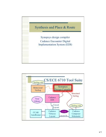
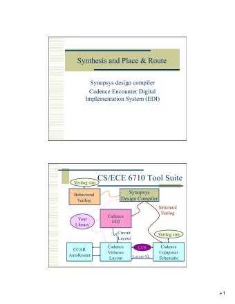
Chip Design with your Cell Library NC_Verilog Synopsys Synthesis Behavioral Verilog Structural Cadence Verilog Your EDI P&R Library NC_Verilog Circuit Spectre Layout Cadence Cadence LVS AutoRouter Virtuoso Composer DRC Layout-XL (EDI or ccar) Layout Schematic Behavioral HDL Description module moore (clk, clr, insig, outsig); / / define combinational logic for input clk, clr, insig; // next_state output outsig; always @(insig or state) // define state encodings as parameters begin parameter [1:0] s0 = 2'b00, case (state) s1 = 2'b01,s2 = 2'b10, s3 = 2'b11; s0: if (insig) next_state = s1; // define reg vars for state register else next_state = s0; // and next_state logic s1: if (insig) next_state = s2; reg [1:0] state, next_state; else next_state = s1; s2: if (insig) next_state = s3; //define state register (with else next_state = s2; //synchronous active-high clear) s3: if (insig) next_state = s1; always @(posedge clk) else next_state = s0; begin endcase if (clr) state = s0; end else state = next_state; // assign outsig as continuous assign end assign outsig = ((state == s1) || (state == s3)); endmodule 18
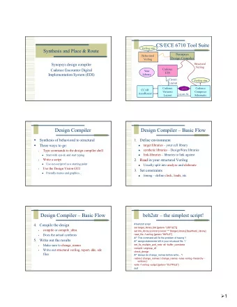
Structural HDL Description Convert the behavioral HDL into a set of logic gates This process is called “synthesis” Synthesis will target the cells (gates) in your library We’ll use Design Compiler from Synopsys Structural HDL Description module moore ( clk, clr, insig, outsig ); input clk, clr, insig; output outsig; wire n4, n5, n6, n7, n8; wire [1:1] state; wire [1:0] next_state; DFF_QB state_reg_0_ ( .D(next_state[0]), .G(clk), .CLR(clr), .Q(outsig), .QB(n4) ); DFF state_reg_1_ ( .D(next_state[1]), .G(clk), .CLR(clr), .Q(state[1]) ); MUX2_INV U7 ( .A(n6), .B(n7), .S(n5), .Y(next_state[1]) ); INVX1 U8 ( .A(state[1]), .Y(n5) ); NAND2 U9 ( .A(outsig), .B(insig), .Y(n7) ); INVX1 U10 ( .A(n4), .Y(n6) ); XOR2 U11 ( .A(insig), .B(n8), .Y(next_state[0]) ); NOR2 U12 ( .A(state[1]), .B(n4), .Y(n8) ); endmodule 19
Assemble Gates into a Circuit Process is called Place and Route We’ll use the Encounter Digital Implementation (EDI) system from Cadence Standard Cells…Power Rings 20
Place Cells and Fillers Connect Rows to Power 21
autoRouted View autoRouted Layout View 22
Corners… Routing 23
Slightly Larger Example And Assemble Whole Chip 24
Example Class Chip (2001) 16-bit Processor, approx 27,000 transistors Same Chip (no M2, M3) 1.5mm x 3.0mm, 72 I/O pads 25
Zoom In… Zoom In… A Hair (100 microns) 26
Recommend
More recommend
Explore More Topics
Stay informed with curated content and fresh updates.

