Slides for Lecture 35 ENEL 353: Digital Circuits Fall 2013 Term - PowerPoint PPT Presentation
Slides for Lecture 35 ENEL 353: Digital Circuits Fall 2013 Term Steve Norman, PhD, PEng Electrical & Computer Engineering Schulich School of Engineering University of Calgary 2 December, 2013 slide 2/33 ENEL 353 F13 Section 02 Slides
Slides for Lecture 35 ENEL 353: Digital Circuits — Fall 2013 Term Steve Norman, PhD, PEng Electrical & Computer Engineering Schulich School of Engineering University of Calgary 2 December, 2013
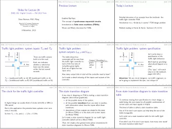
slide 2/33 ENEL 353 F13 Section 02 Slides for Lecture 35 Previous Lecture Counters and shift registers. Introduction to memory arrays.
slide 3/33 ENEL 353 F13 Section 02 Slides for Lecture 35 Today’s Lecture Completion of coverage of memory arrays, including use of ROM circuits to implement combinational logic functions. Related reading in Harris & Harris: Section 5.5
slide 4/33 ENEL 353 F13 Section 02 Slides for Lecture 35 Quick review: The concept of a memory array These are the essential inputs 4 columns Address and outputs of a memory 111 1 0 1 0 array . . . 8 4-bit words in 8 rows 110 0 1 1 1 101 0 0 0 0 N Address Array 100 0 1 1 0 011 1 1 1 1 M 010 0 1 0 0 Data 001 1 1 0 1 For the example at left, with 32 000 0 0 1 1 stored bits, what are N and M?
slide 5/33 ENEL 353 F13 Section 02 Slides for Lecture 35 Bit cells, wordlines, and bitlines Each bit stored within a memory bitline array in stored in a tiny circuit wordline element called a bit cell . stored Signalling to a bit cell is done bit through two wires: a wordline and a bitline . Wordline: Each wordline is connected to all of the bits within a single word. Bitline: Each bitline is connected to all of the bits within a single column. If a memory array has an 8-bit address bus and a 9-bit data bus, how many wordlines are there? How many bitlines?
slide 6/33 ENEL 353 F13 Section 02 Slides for Lecture 35 More about wordlines . . . bitline M − 1 bitline 1 bitline 0 wordline i stored stored stored . . . bit bit bit Each wordline is connected to all of the bits within a single word. Normally one wordline is ON and all the others are OFF, so that a single word is selected for reading or writing. What kind of circuit element is perfectly suited for converting an address input into the correct set of wordline signals?
slide 7/33 ENEL 353 F13 Section 02 Slides for Lecture 35 Organization of a 4 × 3 memory array 2:4 Decoder bitline 2 bitline 1 bitline 0 wordline 3 11 stored stored stored 2 Address bit = 0 bit = 1 bit = 0 wordline 2 10 stored stored stored bit = 1 bit = 0 bit = 0 wordline 1 01 stored stored stored bit = 1 bit = 1 bit = 0 wordline 0 00 stored stored stored bit = 0 bit = 1 bit = 1 Data 2 Data 1 Data 0 Image is Figure 5.42 from Harris D. M. and Harris S. L., Digital Design and Computer Architecture, 2nd ed. , c � 2013, Elsevier, Inc.
slide 8/33 ENEL 353 F13 Section 02 Slides for Lecture 35 Dot notation for ROM circuits 4 columns Address Often a ROM is drawn showing 111 1 0 1 0 only its decoder, the wordlines 8 4-bit words in 8 rows and bitlines, and some dots. 110 0 1 1 1 A dot at a wordline-bitline 101 0 0 0 0 crossing point indicates a 100 0 1 1 0 stored 1 . No dot at a crossing 011 1 1 1 1 point indicates a stored 0 . Let’s draw a dot-notation 010 0 1 0 0 diagram for ROM with the 001 1 1 0 1 contents of the table to the 000 0 0 1 1 right.
slide 9/33 ENEL 353 F13 Section 02 Slides for Lecture 35 ROM-based implementation of logic functions A ROM circuit can be thought of as a “truth table baked into silicon.” This way of thinking about ROM leads to the conclusion that any combinational logic element can be implemented as a ROM circuit. 2 N × M ROM N N M Address C L can be implemented as Data M
slide 10/33 ENEL 353 F13 Section 02 Slides for Lecture 35 ROM-based logic: Examples Let’s implement the following combinational elements using ROM circuits with appropriate dimensions. 1. F = A ⊕ B ; G = ( A ⊕ B ); H = A + B . Let’s do this one by using algebra to express each of F , G , and H as a sum of minterms. 2. E = ABC ; F = A ⊕ B ; G = AB + AC + BC ; H = A + B + C . Let’s do this one by making a truth table.
slide 11/33 ENEL 353 F13 Section 02 Slides for Lecture 35 Why use ROMs for combinational logic? Why not? Using a ROM structure for N -input, M -output logic is sometimes a good design choice, and sometimes not. “Custom” solutions with logic gates tend to use less chip area and less power than ROM-based solutions, and can be much faster. However, the design effort needed for a ROM-based solution is close to zero, so it may be a good choice if area, power, and speed constraints are not pressing.
slide 12/33 ENEL 353 F13 Section 02 Slides for Lecture 35 NMOS transistors NMOS transistors are one of the two main kinds of building blocks drain for CMOS circuits. An NMOS I DS transistor has the four terminals shown, but in CMOS the bulk is gate bulk assumed to be connected to source ground and is usually not shown in circuit diagrams. The relationship of the current I DS to the voltages at the gate, drain and source is quite complex. (See ENCM 467.) But a simple, crude model helps explain how bit cells work in memory arrays.
slide 13/33 ENEL 353 F13 Section 02 Slides for Lecture 35 NMOS transistor with V gate close to zero The first part of our simple, crude model is actually quite accurate. When the gate voltage is close to zero, the drain-to-source connection is like an open switch—no current can flow. drain drain I DS ? I DS = 0 V gate ≈ 0 source source
slide 14/33 ENEL 353 F13 Section 02 Slides for Lecture 35 NMOS transistor with V gate close to V DD The second part of our simple, crude model is not very accurate , but good enough to get a qualitative feel for how bit cells work. When the gate voltage is close to the power supply voltage, the drain-to-source connection is somewhat like a small resistance in series with a closed switch—current flows if V drain � = V source . drain drain I DS ? If V drain � = V source , V gate ≈ V DD then I DS � = 0. source source
slide 15/33 ENEL 353 F13 Section 02 Slides for Lecture 35 A ROM circuit made with NMOS transistors V DD R R R A 2:4 decoder drives the word- line 3 wordlines, but is not shown here, to save word- space on this slide. line 2 What happens to the word- bitlines if wordline 2 is line 1 turned ON and the other three wordlines are OFF? word- line 0 What are the contents of this ROM array? bit- bit- bit- line 2 line 1 line 0
slide 16/33 ENEL 353 F13 Section 02 Slides for Lecture 35 Programmable ROM circuits The ROM circuit on the previous slide can only be made in a semiconductor fab , which is a fancy name for “chip factory”. It’s obviously useful to have circuits that have the essential ROM properties—contents not lost when power is turned off, contents won’t change when normal digital logic voltages are applied—but are also programmable . A programmable ROM is a ROM circuit into which 1’s and 0’s can be written after the circuit is fabricated. See Figure 5.51 and related discussion in Harris & Harris for explanation of one-time-programmable ROM circuits based on fuses that are either blown or intact.
slide 17/33 ENEL 353 F13 Section 02 Slides for Lecture 35 Much cooler than a ROM circuit that can be programmed only once is a ROM circuit that can programmed, then erased, and then re-programmed, many, many times. Production of this kind of erasable, programmable ROM circuit is a huge industry , based on one key electronic device: the floating-gate transistor . Some of the many products that depend utterly on floating-gate transistors are . . . ◮ USB “thumb” drives ◮ SD cards and related storage techologies ◮ solid-state drives in laptop and desktop computers ◮ smartphones and tablet computers Some slides at the end of this slide set give a brief explanation of floating-gate transistor behaviour.
slide 18/33 ENEL 353 F13 Section 02 Slides for Lecture 35 What’s left in ENEL 353 in Fall 2013? Tutorial Tue Dec 3. Problems on some or all of the following topics: FSMs, timing constraints with clock skew, counters, shift registers, memory arrays. Examinable material in lecture Wed Dec 4. PLAs (Harris and Harris Section 5.6.1). Non-examinable material in lecture Wed Dec 4. Topics are yet to be determined. Lecture Fri Dec 6. Comments about the final exam, and review of course content.
This is the end point for material I am committed to presenting in the lecture period. The remaining slides try to briefly explain how RAM circuits and EEPROM (electrically-erasable programmable ROM) circuits work, and are not examinable material.
slide 20/33 ENEL 353 F13 Section 02 Slides for Lecture 35 How writes and read work in RAM circuits The next few slides attempt to give a rough explanation of how data is written into and read out of bits cells in a RAM array. It’s hard to give a really detailed explanation without referring to ideas about transistors and circuit theory that come later than Fall Term of Year 2 in the ENEL degree program. The next slide shows a hypothetical 4 × 3 RAM array. Keep in mind that practical RAM circuits are much, much larger, with thousands, millions, or even billions of bit cells. A lot of the circuit design issues have to with the fact that bit cells are tiny, not-very-powerful circuits, while bitlines are relatively lengthy pieces of metal. It’s not possible for a single bit cell to quickly drive the voltage on a bitline all the way from LOW to HIGH or HIGH to LOW.
Recommend
More recommend
Explore More Topics
Stay informed with curated content and fresh updates.
![MARKDOWN SLIDES [EN] MARKDOWN SLIDES [EN] MARKDOWN SLIDES [EN] MARKDOWN SLIDES [EN] MARKDOWN](https://c.sambuz.com/818511/markdown-slides-en-markdown-slides-en-markdown-slides-en-s.webp)




![1 Mor M. Peretz, Switch-Mode Power Supplies [7-4] Miller effect V o C gd R g G I g V s C gs](https://c.sambuz.com/991519/1-s.webp)
