Slides for Lecture 34 ENEL 353: Digital Circuits Fall 2013 Term - PowerPoint PPT Presentation
Slides for Lecture 34 ENEL 353: Digital Circuits Fall 2013 Term Steve Norman, PhD, PEng Electrical & Computer Engineering Schulich School of Engineering University of Calgary 29 November, 2013 slide 2/20 ENEL 353 F13 Section 02
Slides for Lecture 34 ENEL 353: Digital Circuits — Fall 2013 Term Steve Norman, PhD, PEng Electrical & Computer Engineering Schulich School of Engineering University of Calgary 29 November, 2013
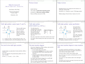
slide 2/20 ENEL 353 F13 Section 02 Slides for Lecture 34 Previous Lecture The problem of asynchronous inputs to synchronous systems; solution with synchronizer circuits. Some insight into where metastability and setup times come from.
slide 3/20 ENEL 353 F13 Section 02 Slides for Lecture 34 Today’s Lecture Counters and shift registers. Introduction to memory arrays. Related reading in Harris & Harris: Sections 5.4 and 5.5.
slide 4/20 ENEL 353 F13 Section 02 Slides for Lecture 34 Counters Counter is a name used for any kind of synchronous sequential circuit designed to move one step per clock cycle through some specified counting sequence . There is a huge variety of kinds of counters, such as ◮ N-bit binary counters , which count from 0 up to 2 N − 1, then return to 0; ◮ decade counters , which count from 0 up to 9, then return to 0; ◮ down-counters , which go to some maximum value on reset, then count down to 0. We’ve already seen lots of counters in lectures, Lab 4, and Problem Set 5, so it’s best to spend our remaining lecture time on other topics.
slide 5/20 ENEL 353 F13 Section 02 Slides for Lecture 34 Shift registers Shift register is a name used for a synchronous sequential circuit made from a chain of flip-flops . In normal operation of a shift register, a typical D input to DFF is driven by the Q output of a neighbouring DFF. Although the name shift register hasn’t been used, shift registers have already appeared a few times in ENEL 353. For example, the divide-by-3 counter with one-hot state encoding stores its state in a shift register. Two of the many practical applications of shift registers are parallel-to-serial conversion and serial-to-parallel conversion.
slide 6/20 ENEL 353 F13 Section 02 Slides for Lecture 34 serial and parallel N -bit parallel data communication uses N wires to transmit N bits at the same time. Most data communication within a computer processor circuit is parallel. Serial data communication transmits one bit per time interval. Often the time interval is one system clock period. An example of serial communication is the Universal Serial Bus (USB) system, which is very widely used to connect computers to peripherals such as printers, keyboards, and many kinds of external storage devices.
slide 7/20 ENEL 353 F13 Section 02 Slides for Lecture 34 Universal Serial Bus USB connections—version 2.0 and earlier—have 4 wires: ◮ 5V and ground for powering devices; ◮ two wires for serial communication—a 1 or 0 is transmitted as a voltage difference between these two wires. (Public domain photo taken from Wikipedia article on USB.)
slide 8/20 ENEL 353 F13 Section 02 Slides for Lecture 34 N -bit parallel-in-serial-out shift register N bits can be copied into the shift register in a single clock cycle. The bits come out one at a time over N clock cycles. Here’s an example with N = 4. It should be pretty obvious how to redesign the circuit for some value of N that isn’t 4 . . . A 0 A 1 A 2 A 3 CLK 1 1 1 1 Y = Q 3 0 0 0 0 Q 0 Q 1 Q 2 Load When Load = 1, the DFFs do a “parallel load”, copying A N − 1:0 on a rising edge of CLK. When Load = 0, the DFFs copy their neighbour’s outputs: Q ′ k = Q k − 1 for 0 < k < N .
slide 9/20 ENEL 353 F13 Section 02 Slides for Lecture 34 A 0 A 1 A 2 A 3 CLK 1 1 1 1 Y = Q 3 0 0 0 0 Q 0 Q 1 Q 2 Load Suppose Q 3:0 = 0000 just before time t 0 . Let’s complete the timing diagram . . . CLK Load 1101 A 3:0 Q 3:0 Y t 0
slide 10/20 ENEL 353 F13 Section 02 Slides for Lecture 34 When is it time to load more parallel data? A 0 A 1 A 2 A 3 CLK 1 1 1 1 Y = Q 3 0 0 0 0 Q 0 Q 1 Q 2 Load Let’s suppose we’ve built the above circuit, but with N = 8 instead of N = 4. So there are 8 parallel inputs ( A 7:0 ), 8 multiplexers, and 8 DFFs. What would be a useful “companion circuit”, that could request a new parallel load after all eight bits from the previous load have been copied out on Y ?
slide 11/20 ENEL 353 F13 Section 02 Slides for Lecture 34 N -bit serial-in-parallel-out shift register Here’s an example with N = 4. Note the use of DFFs with enable inputs. CLK Q 0 Q 1 Q 2 Q 3 A EN EN EN EN Shift Y 0 Y 1 Y 2 Y 3 When Shift = 1, data arriving on A , one bit per clock cycle, gets copied into the shift register. When Shift = 0, the shift register is frozen, allowing a parallel transfer of the data on Y N − 1:0 . For the circuit to work correctly, what must be true about the signals A and CLK?
slide 12/20 ENEL 353 F13 Section 02 Slides for Lecture 34 Memory arrays A memory array is a digital N Address Array circuit element connected to an N -bit address bus , an M -bit data bus , and most M likely some other signals. Data The address bus is unidirectional—it’s always an input to the array. The data bus is bidirectional—an input when the array is written to , an output when the array is read from . Inside the array there are 2 N × M stored bits .
slide 13/20 ENEL 353 F13 Section 02 Slides for Lecture 34 Stored bits in a memory array 4 columns Address Here is an example with N = 3 and 111 1 0 1 0 M = 4. 8 4-bit words in 8 rows 110 0 1 1 1 There are 2 N = 2 3 = 8 different 101 0 0 0 0 possible addresses. At each address 100 0 1 1 0 there is a stored 4-bit word . 011 1 1 1 1 This example would be called an 010 0 1 0 0 8 × 4 array . In this example, 8 is the 001 1 1 0 1 depth and 4 is the width . The width is sometimes called the word size . 000 0 0 1 1 Of course the 0’s and 1’s are not really stored as tiny pictures of the characters 0 and 1! Different kinds of memory arrays use different kinds of circuit elements to hold 0’s and 1’s.
slide 14/20 ENEL 353 F13 Section 02 Slides for Lecture 34 An example of a larger array Tiny arrays like the one on the previous slide are good for textbook and lecture examples, and there are also some practical uses for such small arrays. However, memory arrays can be much larger. Suppose N , the address size, is 16 bits, and M , the data size (word size) is 8 bits. ◮ What are the dimensions of the memory array? ◮ How many bits are stored in the array?
slide 15/20 ENEL 353 F13 Section 02 Slides for Lecture 34 ROM and RAM: Names we’re stuck with, part 1 These not-particularly-descriptive names have been around for decades, and are unlikely to change any time soon. ROM stands for “read-only memory”. It’s true that ROM is read-only, when voltages between 0 and V DD are applied. (Some ROM circuits are writeable if voltages outside of the 0-to- V DD range are applied!) But it’s also true and just as important that ROM is nonvolatile : In ROM, stored 0’s and 1’s are preserved when the power is off. A more descriptive name for “ROM circuit” would be NVMA: nonvolatile memory array.
slide 16/20 ENEL 353 F13 Section 02 Slides for Lecture 34 ROM and RAM: Names we’re stuck with, part 2 RAM stands for “random access memory”. Random access means that access to any one word in an array is no faster and no slower than access to any other word. Mass storage devices such as magnetic disk drives, magnetic tape drives, and CD/DVD/Blu-ray drives do not have this random access property. But ROM circuits are random access, which makes RAM a silly name for something that is different in important ways from ROM!
slide 17/20 ENEL 353 F13 Section 02 Slides for Lecture 34 ROM and RAM: Names we’re stuck with, part 3 The key properties of a RAM array are: ◮ it is both readable and writeable, using voltages in the 0-to- V DD range; ◮ it is volatile —all the stored 0’s and 1’s are lost when power is turned off. A very precise but somewhat unpronounceable name for “RAM circuit” would be VRWMA (volatile readable/writeable memory array). Your instructor seriously doubts that “VRWMA” will replace “RAM circuit” as a name any time in the near future!
slide 18/20 ENEL 353 F13 Section 02 Slides for Lecture 34 ROM compared to RAM N Address 1-port 1-port N Address ROM WE RAM Array ? Array other signals M M Data Data WE stands for “write enable”. WE = 1 tells RAM to write to the word specified by Address, and WE = 0 tells RAM to read from the word specified by Address. Which array is combinational logic and which is sequential? Is the sequential circuit synchronous or asynchronous?
slide 19/20 ENEL 353 F13 Section 02 Slides for Lecture 34 How many ports? N Address 1-port 1-port N Address ROM WE RAM Array ? Array other signals M M Data Data The circuits above are called “1-port” because at any given time, the array can receive only one address and can support only one read or write operation. See Harris & Harris for an example of a 3-port memory array, which can support two read operations and one write operation all at one time, possibly involving three different addresses.
slide 20/20 ENEL 353 F13 Section 02 Slides for Lecture 34 What’s left in ENEL 353? Definitely this topic: ◮ More about memory arrays (H&H Section 5.5). As time permits, some or all of these topics: ◮ PLAs (H&H Section 5.6.1). ◮ Carry-lookahead adders (H&H Section 5.2.1). ◮ Subtractors (H&H Section 5.2.2).
Recommend
More recommend
Explore More Topics
Stay informed with curated content and fresh updates.
![MARKDOWN SLIDES [EN] MARKDOWN SLIDES [EN] MARKDOWN SLIDES [EN] MARKDOWN SLIDES [EN] MARKDOWN](https://c.sambuz.com/818511/markdown-slides-en-markdown-slides-en-markdown-slides-en-s.webp)


