Slides for Lecture 24 ENEL 353: Digital Circuits Fall 2013 Term - PowerPoint PPT Presentation
Slides for Lecture 24 ENEL 353: Digital Circuits Fall 2013 Term Steve Norman, PhD, PEng Electrical & Computer Engineering Schulich School of Engineering University of Calgary 4 November, 2013 slide 2/17 ENEL 353 F13 Section 02 Slides
Slides for Lecture 24 ENEL 353: Digital Circuits — Fall 2013 Term Steve Norman, PhD, PEng Electrical & Computer Engineering Schulich School of Engineering University of Calgary 4 November, 2013
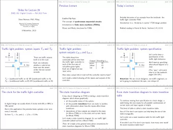
slide 2/17 ENEL 353 F13 Section 02 Slides for Lecture 24 Previous Lecture Clock signals in digital circuits. D latches. Introduction to D flip-flops.
slide 3/17 ENEL 353 F13 Section 02 Slides for Lecture 24 Today’s Lecture Building a D flip-flop out of two D latches in a “master-slave” configuration. The clock divider circuit—a simple application of a D flip-flop. Registers—storing multiple bits in collection of D flip-flops. Enabled flip-flops and resettable flip-flops. Related reading in Harris & Harris: Sections 3.2.3–3.2.6, 3.2.8
slide 4/17 ENEL 353 F13 Section 02 Slides for Lecture 24 A good quote from your textbook (repeat slide) From page 114 of Harris and Harris: A D flip-flop copies D to Q on the rising edge of the clock, and remembers its state at all other times. Reread this definition until you have it memorized; one of the most common problems for beginning digital designers is to forget what a flip-flop does.
slide 5/17 ENEL 353 F13 Section 02 Slides for Lecture 24 D flip-flop implementation using two D latches: “master-slave” configuration CLK input for flip-flop Your instructor thinks that grabber-holder would be a more descriptive (and less creepy) name than CLK CLK master-slave for this kind N1 D IN Q OUT D Q D Q of D flip-flop design. Q Q Let’s make some notes on master slave the jobs done by the master latch latch and slave latches in this D flip-flop circuit.
CLK input for flip-flop slide 6 CLK CLK N1 D IN Q OUT D Q D Q Q Q master slave latch latch D flip-flop Let’s see how this circuit works by completing this diagram . . . 1 flip-flop CLK 0 1 D IN 0 1 N1 0 1 Q OUT 0
The clock divider slide 7 This simple and useful circuit CLK1 can be built with a D flip-flop and an inverter. The output D Q CLK2 CLK2 is a clock signal with half the frequency of the input CLK1. If the frequency of CLK1 is, say, 100 kHz, the signals will look like this on an oscilloscope . . . CLK1 CLK2 The basic behaviour of a D flip-flop explains why CLK2 is constant between rising edges of CLK1. But what is going on at those rising edges? According to the inverter, D = Q , but according to the flip-flop Q = D . It seems like D has to be 0 and 1 at the same time!
slide 8/17 ENEL 353 F13 Section 02 Slides for Lecture 24 How the clock divider works We already know that the inverter has a minimum CLK1 delay t cd . The flip-flop is a physical D Q CLK2 device, so also has a minimum delay, which is called t ccq . Let’s make some notes about t ccq . Now let’s study what happens when Q = 0 just before a rising edge of CLK1, and when Q = 1 just before a rising edge of CLK1.
slide 9/17 ENEL 353 F13 Section 02 Slides for Lecture 24 A small amount of delay is a good thing! We’ve just seen that delays in the clock divider circuit are essential in making it work. The same idea is true for most other systems built using D flip-flops. Of course, long delays are bad —they result in circuits that are slow or unreliable, or both. Note: There is much more to learn about timing of flip-flop circuits, but we won’t do that until we get to Section 3.5 of Harris & Harris.
slide 10/17 ENEL 353 F13 Section 02 Slides for Lecture 24 About the clock edges visible on the ’scope . . . A few slides back it was suggested that if the clock divider input frequency was 100 kHz, the input and output signals would look like this on an oscilloscope . . . CLK1 CLK2 Why do all the clock edges appear to be perfectly vertical? Why do the edges on CLK2 appear to occur at exactly the same time as rising edges on CLK1?
slide 11/17 ENEL 353 F13 Section 02 Slides for Lecture 24 Abbreviations for “D flip-flop” DFF is short, simple and obvious, so we’ll use it in this course. Some literature uses the term flop , which is short but possibly ambiguous.
slide 12/17 ENEL 353 F13 Section 02 Slides for Lecture 24 Symbols for D flip-flops In symbols, the triangle on the CLK input indicates an edge-triggered device. With Q Lacking Q Lacking Q output . . . output . . . output, condensed CLK CLK symbol . . . CLK D Q D Q D Q Q All DFF designs have an internal Q signal, but many of them, to save space and power, do not make Q available as an output.
slide 13/17 ENEL 353 F13 Section 02 Slides for Lecture 24 N -bit registers CLK An N -bit register is a group of D 3 D Q Q 3 N DFFs with a common CLK input. At right, (a) shows 4 DFFs D 2 D Q Q 2 configured as a 4-bit register, and (b) is a symbol for that D 1 D Q Q 1 register. Let’s make some notes about CLK D 0 D Q Q 0 the symbol. 4 4 D 3:0 Q 3:0 (a) (b) Image is taken from Figure 3.9 from Harris D. M. and Harris S. L., Digital Design and Computer Architecture, 2nd ed. , c � 2013, Elsevier, Inc.
slide 14/17 ENEL 353 F13 Section 02 Slides for Lecture 24 Enabled D flip-flops D Q EN This kind of DFF is good for a circuit design in which it is useful to have a flip-flop sometimes hold its state for many clock cycles, rather than copy D on every single rising edge of the clock. Let’s write a precise description of the behaviour of an enabled DFF. Let’s show how an enabled DFF can be built using a “plain” DFF and a 2:1 multiplexer.
slide 15/17 ENEL 353 F13 Section 02 Slides for Lecture 24 Resettable D flip-flops Here are two symbols for the same thing . . . D Q r RESET Let’s write a precise description of the behaviour of a resettable DFF, then build one using a “plain” DFF, an AND gate, and an inverter What would DFFs with reset inputs be useful for?
slide 16/17 ENEL 353 F13 Section 02 Slides for Lecture 24 The rest of Section 3.2 in Harris & Harris Section 3.2.7 presents and explains the most common present-day transistor-level designs for D latches and DFFs. We will not cover this topic in ENEL 353. If you are curious about this material, you will have to go back and read Section 1.7 before reading Section 3.2.7. Section 3.2.8 has a good example illustrating the difference between a D latch and a DFF. Check it out carefully!
slide 17/17 ENEL 353 F13 Section 02 Slides for Lecture 24 Upcoming topics The concept of synchronous sequential circuits . Introduction to finite state machines . Related reading in Harris & Harris: Section 3.3; Section 3.4 to the end of Section 3.4.1.
Recommend
More recommend
Explore More Topics
Stay informed with curated content and fresh updates.
![MARKDOWN SLIDES [EN] MARKDOWN SLIDES [EN] MARKDOWN SLIDES [EN] MARKDOWN SLIDES [EN] MARKDOWN](https://c.sambuz.com/818511/markdown-slides-en-markdown-slides-en-markdown-slides-en-s.webp)


