Slides for Lecture 13 ENEL 353: Digital Circuits Fall 2013 Term - PowerPoint PPT Presentation
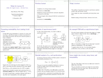
Slides for Lecture 13 ENEL 353: Digital Circuits Fall 2013 Term Steve Norman, PhD, PEng Electrical & Computer Engineering Schulich School of Engineering University of Calgary 7 October, 2013 slide 2/17 ENEL 353 F13 Section 02 Slides
Slides for Lecture 13 ENEL 353: Digital Circuits — Fall 2013 Term Steve Norman, PhD, PEng Electrical & Computer Engineering Schulich School of Engineering University of Calgary 7 October, 2013
slide 2/17 ENEL 353 F13 Section 02 Slides for Lecture 13 Previous Lecture A little more about drawing schematics. The concept of a minimal SOP expression. Multilevel combinational logic. Simple models for CMOS logic gates—useful for understanding unknown/illegal (X) and floating/high-impedance (Z) values in combinational logic.
slide 3/17 ENEL 353 F13 Section 02 Slides for Lecture 13 Today’s Lecture Completion of material on X and Z values at nodes of logic circuits. Introduction to Karnaugh maps (also known as K-maps ). Related reading in Harris & Harris: Sections 2.6 and 2.7 (up to the end of 2.7.2).
slide 4/17 ENEL 353 F13 Section 02 Slides for Lecture 13 Simple model for a CMOS gate with LOW output (This slide is a repeat from the previous lecture.) V DD pull-up network is OFF . . . near INFINITE resistance inputs output pull-down network is ON . . . SMALL resistance GND The actual behaviour of the transistors inside the pull-up and pull-down networks is more complicated than this model suggests!
slide 5/17 ENEL 353 F13 Section 02 Slides for Lecture 13 Simple model for a CMOS gate with HIGH output (Another repeat from the previous lecture.) V DD pull-up network is ON . . . SMALL resistance inputs output pull-down network is OFF . . . near INFINITE resistance GND Again, real circuit behaviour is not quite this simple.
slide 6/17 ENEL 353 F13 Section 02 Slides for Lecture 13 What happens if two or more gate outputs are wired together? Usually, this is a bad thing to do. Let’s use our simple model for CMOS gates to understand what happens when Gate A is trying to output a 1 and Gate B is trying to output a 0 in this circuit . . . gate A gate inputs A gate B gate What’s the voltage inputs B at this node? Note: For some special kinds of gates, it is actually useful to wire gate outputs to each other.
slide 7/17 ENEL 353 F13 Section 02 Slides for Lecture 13 Illegal value: X at a node rather than 0 or 1 The symbol X is used to indicate that a node has an illegal or unknown value. Complex digital designs written in hardware description languages like VHDL or SystemVerilog can be tested for correctness using logic simulator software . A logic simulator would use X to represent the gate A/gate B output for the situation in the previous slide. An X value for a node in a simulation result could also indicate one of many other kinds of defect in the circuit being simulated.
slide 8/17 ENEL 353 F13 Section 02 Slides for Lecture 13 Warning: There’s another meaning for X in digital logic We’ll soon see that X is also used to indicate don’t care value in some truth tables and Karnaugh maps. X for don’t care does not mean the same thing as X for illegal/unknown value. It’s unfortunate that X has two different meanings. X for illegal/unknown value is used as a possible state of a node in a specific circuit design . We’ll soon discover that X for don’t-care shows up in some truth tables and Karnaugh maps corresponding to those truth tables.
slide 9/17 ENEL 353 F13 Section 02 Slides for Lecture 13 What if pull-up and pull-down networks are BOTH OFF? Most logic gates are V DD designed to switch between one of two OFF: near-infinite resistance states: inputs output ◮ pull-up OFF, pull-down ON OFF: near-infinite resistance ◮ pull-up ON, pull-down OFF GND However, some special kinds of gates can go into the state shown in the diagram, in response to certain input combinations. What can we say about the output node in this situation?
slide 10/17 ENEL 353 F13 Section 02 Slides for Lecture 13 Tristate buffers A tristate buffer has two inputs, often called A and E — E is for enable . (Sometimes the enable signal gets the two-letter symbol EN.) Here are the logic symbol and a table showing what the pull-up and pull-down networks do for all possible input combinations: E A pull-up pull-down E 0 0 OFF OFF 0 1 OFF OFF A Y 1 0 OFF ON 1 1 ON OFF Let’s use the table to describe in words how a tristate buffer behaves.
slide 11/17 ENEL 353 F13 Section 02 Slides for Lecture 13 An application of tristate buffers common output E 1 The goal of this design is wire that sometimes gate 1 gate 1 will control the common output wire, sometimes inputs E 2 gate 2 will be in control, and so on. gate 2 To meet this goal, what . . . . . . has to be true about the E N logic driving the signals E 1 , E 2 , . . . , E N ? gate N
slide 12/17 ENEL 353 F13 Section 02 Slides for Lecture 13 Karnaugh Maps A Karnaugh map , often called a “K-map”, is a representation of a truth table as a two-dimensional grid of cells—each cell represents a single row of the truth table. K-maps can be used to quickly find minimal SOP expressions for logic functions. A simple trick allows use of K-maps to find minimal POS expressions as well. The next slide is a preview example of the use of K-maps. You’re not expected to understand all of it today, but you can probably make some good guesses about what is going on . . .
A B C D F K-map for F : 0 0 0 0 0 0 0 0 1 1 A A B 0 0 1 0 0 00 01 11 10 C D 0 0 1 1 1 00 0 1 0 0 0 0 1 0 1 0 01 1 1 1 0 1 1 0 1 D 0 1 1 1 1 11 1 1 1 C 1 0 0 0 0 10 1 1 0 0 1 1 1 0 1 0 0 B 1 0 1 1 1 1 1 0 0 0 Minimal SOP expression for F : 1 1 0 1 1 1 1 1 0 0 BD + ¯ ¯ ABC + A ¯ CD 1 1 1 1 0
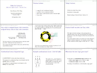
slide 14/17 ENEL 353 F13 Section 02 Slides for Lecture 13 K-map preliminaries: Gray code ordering For K-maps to work correctly, rows and columns must use Gray code ordering. It’s not an option! The one-bit Gray code sequence is trivial: 0, 1. The two-bit Gray code sequence is simple, and you should commit it to memory: 00, 01, 11, 10. Remember, only one bit can change as you go from one code word to the next. It’s easy to slip up, because after you write a lot of 2-input truth tables, the 2-bit unsigned binary code sequence (00, 01, 10, 11) appears in your mind almost automatically. Memorize this: Two-bit Gray code: zero, one, three, two!
slide 15/17 ENEL 353 F13 Section 02 Slides for Lecture 13 Preliminaries: Layout of 3- and 4-variable maps With 3 variables, you can choose either a “wide” layout or a “tall” layout. With 4 variables, the only reasonable layout is a square of 16 cells. A A A B 0 1 00 01 11 10 B C C D A A B 00 00 00 01 11 10 C 0 01 01 D C 1 11 11 B C B 10 10 B Let’s make some further notes about K-map layouts.
slide 16/17 ENEL 353 F13 Section 02 Slides for Lecture 13 From truth table rows to K-map 1-cells Each row of the truth table for a function F in which F = 1 generates a 1-cell in the K-map Foo Bar Quux F of F . The values of the inputs 0 0 0 0 in a truth table row give you 0 0 1 0 K-map row and column 0 1 0 1 numbers for the 1-cell. 0 1 1 1 For truth table rows in which 1 0 0 0 F = 0, K-map cells are often 1 0 1 0 left blank . (Harris & Harris 1 1 0 0 put 0’s in those cells.) 1 1 1 1 For the example F on this slide, let’s lay out a K-map and mark the 1-cells.
slide 17/17 ENEL 353 F13 Section 02 Slides for Lecture 13 Upcoming topics K-map terminology: implicant , prime implicant , distinguished 1-cell , essential prime implicant . Using K-maps to find minimal SOP expressions for functions. Related reading in Harris & Harris: Sections 2.7, up to the end of Section 2.7.2.
Recommend
More recommend
Explore More Topics
Stay informed with curated content and fresh updates.
![MARKDOWN SLIDES [EN] MARKDOWN SLIDES [EN] MARKDOWN SLIDES [EN] MARKDOWN SLIDES [EN] MARKDOWN](https://c.sambuz.com/818511/markdown-slides-en-markdown-slides-en-markdown-slides-en-s.webp)

