Present Status and Future Direction of BSIM SOI Model for High- - PDF document
Present Status and Future Direction of BSIM SOI Model for High- Performance/Low-Power/RF Application Samuel K. H. Fung, *Pin Su, *Chenming Hu IBM Microelectronics, Semiconductor Research and Development Center (SRDC), Hopewell Junction, New York
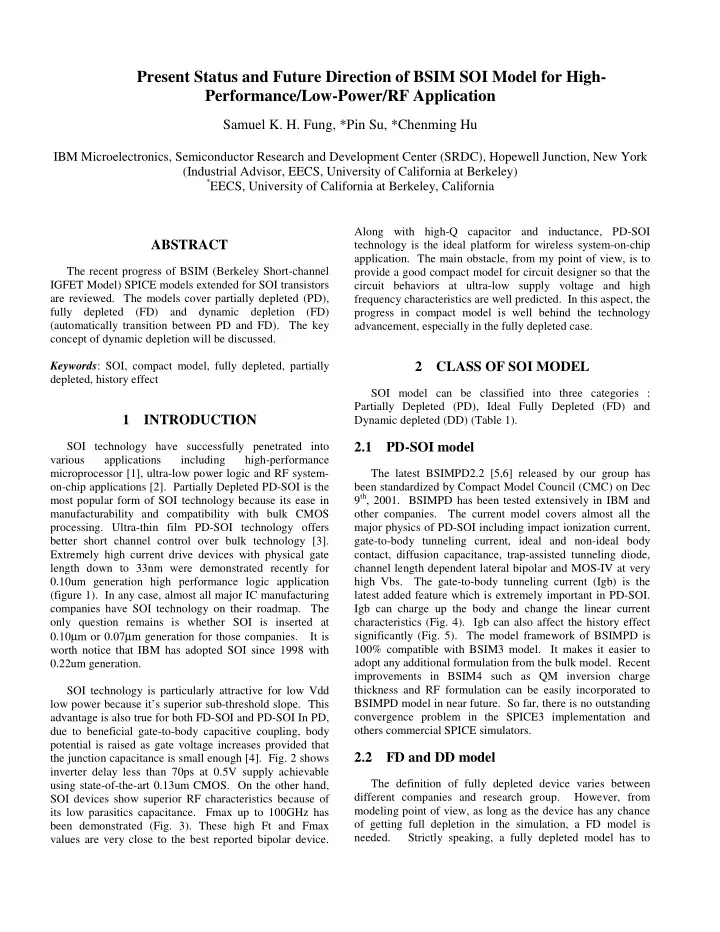
Present Status and Future Direction of BSIM SOI Model for High- Performance/Low-Power/RF Application Samuel K. H. Fung, *Pin Su, *Chenming Hu IBM Microelectronics, Semiconductor Research and Development Center (SRDC), Hopewell Junction, New York (Industrial Advisor, EECS, University of California at Berkeley) * EECS, University of California at Berkeley, California Along with high-Q capacitor and inductance, PD-SOI ABSTRACT technology is the ideal platform for wireless system-on-chip application. The main obstacle, from my point of view, is to The recent progress of BSIM (Berkeley Short-channel provide a good compact model for circuit designer so that the IGFET Model) SPICE models extended for SOI transistors circuit behaviors at ultra-low supply voltage and high are reviewed. The models cover partially depleted (PD), frequency characteristics are well predicted. In this aspect, the fully depleted (FD) and dynamic depletion (FD) progress in compact model is well behind the technology (automatically transition between PD and FD). The key advancement, especially in the fully depleted case. concept of dynamic depletion will be discussed. Keywords : SOI, compact model, fully depleted, partially 2 CLASS OF SOI MODEL depleted, history effect SOI model can be classified into three categories : Partially Depleted (PD), Ideal Fully Depleted (FD) and 1 INTRODUCTION Dynamic depleted (DD) (Table 1). SOI technology have successfully penetrated into 2.1 PD-SOI model various applications including high-performance microprocessor [1], ultra-low power logic and RF system- The latest BSIMPD2.2 [5,6] released by our group has on-chip applications [2]. Partially Depleted PD-SOI is the been standardized by Compact Model Council (CMC) on Dec 9 th , 2001. BSIMPD has been tested extensively in IBM and most popular form of SOI technology because its ease in manufacturability and compatibility with bulk CMOS other companies. The current model covers almost all the processing. Ultra-thin film PD-SOI technology offers major physics of PD-SOI including impact ionization current, better short channel control over bulk technology [3]. gate-to-body tunneling current, ideal and non-ideal body Extremely high current drive devices with physical gate contact, diffusion capacitance, trap-assisted tunneling diode, length down to 33nm were demonstrated recently for channel length dependent lateral bipolar and MOS-IV at very 0.10um generation high performance logic application high Vbs. The gate-to-body tunneling current (Igb) is the (figure 1). In any case, almost all major IC manufacturing latest added feature which is extremely important in PD-SOI. companies have SOI technology on their roadmap. The Igb can charge up the body and change the linear current only question remains is whether SOI is inserted at characteristics (Fig. 4). Igb can also affect the history effect 0.10 µ m or 0.07 µ m generation for those companies. significantly (Fig. 5). The model framework of BSIMPD is It is worth notice that IBM has adopted SOI since 1998 with 100% compatible with BSIM3 model. It makes it easier to adopt any additional formulation from the bulk model. Recent 0.22um generation. improvements in BSIM4 such as QM inversion charge thickness and RF formulation can be easily incorporated to SOI technology is particularly attractive for low Vdd low power because it’s superior sub-threshold slope. This BSIMPD model in near future. So far, there is no outstanding convergence problem in the SPICE3 implementation and advantage is also true for both FD-SOI and PD-SOI In PD, others commercial SPICE simulators. due to beneficial gate-to-body capacitive coupling, body potential is raised as gate voltage increases provided that 2.2 FD and DD model the junction capacitance is small enough [4]. Fig. 2 shows inverter delay less than 70ps at 0.5V supply achievable The definition of fully depleted device varies between using state-of-the-art 0.13um CMOS. On the other hand, different companies and research group. However, from SOI devices show superior RF characteristics because of modeling point of view, as long as the device has any chance its low parasitics capacitance. Fmax up to 100GHz has of getting full depletion in the simulation, a FD model is been demonstrated (Fig. 3). These high Ft and Fmax needed. Strictly speaking, a fully depleted model has to values are very close to the best reported bipolar device.
Recommend
More recommend
Explore More Topics
Stay informed with curated content and fresh updates.
