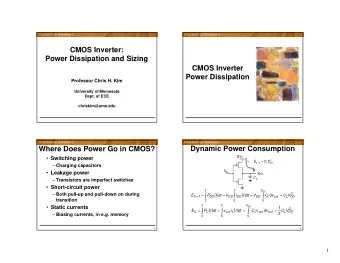
Ultimately Scaled CMOS: DG FinFETs? Jerry G. Fossum SOI Group - PowerPoint PPT Presentation
Ultimately Scaled CMOS: DG FinFETs? Jerry G. Fossum SOI Group Department of Electrical and Computer Engineering University of Florida Gainesville, FL 32611-6130 J. G. Fossum / 1 Outline Introduction - CMOS Scaling Thin-BOX FD/SOI
Ultimately Scaled CMOS: DG FinFETs? Jerry G. Fossum SOI Group Department of Electrical and Computer Engineering University of Florida Gainesville, FL 32611-6130 J. G. Fossum / 1
Outline ❋ Introduction - CMOS Scaling ❋ Thin-BOX FD/SOI MOSFETs ❋ Pragmatic Nanoscale FinFETs ❋ Conclusions J. G. Fossum / 2
Projected HP CMOS Gate-Length Scaling * [Intel: bulk-Si MOSFETs] 7nm [6nm in 2020!] * 2003 SIA ITRS J. G. Fossum / 3
Contemporary Bulk-Silicon MOSFET N B (x,y) Substrate/Well Body Has been scaled a la Moore’s (and now, “More than Moore”) Law, but with increasingly complex boosters and body/channel doping density N B , which can no longer (i.e., for L g < ~30nm) be adequately controlled. J. G. Fossum / 4
Continued Scaling to L g < 10nm: Undoped UTBs/Channels (n)FinFET on SOI? FD/SOI (n)MOSFET w/ thin BOX and GP? Gate Gate Gf n + n + p - STI BOX STI p + GP Si Substrate n+ n+ n+ n+ Source Source Drain Drain NO. Complex processing/layout. BOX YES. Selective GPs, w/ biasing. Tuned dual-metal gate work functions. Quasi-planar. High inherent V t : Conventional processing, w/o N B . ( )φ c ∼ V t long = 1 + r 0.6 V . Two gates: good SCE control. ( ) Can be pragmatic. J. G. Fossum / 5
2-D Numerical Simulations: Projected Scaling Limits Taurus-predicted LP and HP scaling limits (L eff , which, with G-S/D underlap, can be 5-10nm longer than L g ), defined by t Si = 5nm, for thin-BOX/GP nMOSFETs and DG nFinFETs. The devices have been designed for I off ~ 10pA/ µ m and ~100nA/ µ m for LP and HP applications, respectively, with DIBL ≤ 100mV/V. The 18nm limit for the HP thin-BOX/GP device with V GP is questionable due to the very large ∆Φ Gf (gate work-function tuning below midgap) needed; the scaling limit of 25nm without V GP is more realistic. Thin-BOX/GP Thin-BOX/GP LP DG FinFET w/o V GP w/ V GP L eff (nm) 28 18 25/ 15 ∆Φ Gf (mV) 0 450 0/-450 Thin-BOX/GP Thin-BOX/GP HP DG FinFET w/o V GP w/ V GP L eff (nm) 25 18? 15 ∆Φ Gf (mV) 0 850 0 Pragmatic FinFET-CMOS can be scaled to the end of the SIA ITRS. J. G. Fossum / 6
Nanoscale Pragmatic-FinFET CMOS ❋ On SOI (no isolation, S-D leakage complexities). ❋ Undoped fin-UTB/channel (no RDF effects). ❋ DG, not TG (a top gate is virtually ineffective). ❋ One ~midgap metal gate (for nMOS and pMOS). ❋ No channel strain (mobilities are high without it). ❋ No high-k dielectric (relatively thick SiON is OK). ❋ G-S/D underlap (L eff(weak) > L g , L eff(strong) ≅ L g ). ❋ S/D processing for V t control (and underlap). J. G. Fossum / 7
The optimal number of gates is 2! Davinci (3-D): Undoped L eff = 28nm TG fin size for SCE control; t ox = 1.1nm 2.0 S = 80mV DIBL = 100mV/V 1.5 h Si /L eff 1.0 h Si = w Si = L eff DG h Si = w Si ( ⇒ easier fin) 0.5 1/5 ~ h Si(FD) /L eff Design Space FD/SOI 0.0 0.0 0.5 1.0 1.5 2.0 w Si /L eff w Si(DG) /L eff ~ 1/2 Two gates (DG) give good control of electrostatics (i.e., SCEs) with thicker UTB than that needed for one-gate (FD/SOI) device. J. G. Fossum / 8
A third (top) gate is not very beneficial ... Davinci (w/o QM): L eff = 25nm, w Si = 13nm, t ox = 1.2nm 100 60 TG FinFET 80 50 DG FinFET ∆ I on /I on(DG) (%) R f ≡ h Si /w Si = 3 40 60 I DS ( µ A) 30 40 20 W eff -implied 20 [w Si /(2h Si )] 10 V DS =1.0V 0 0 0.5 1.0 1.5 2.0 2.5 3.0 3.5 4.0 4.5 5.0 5.5 0.2 0.3 0.4 0.5 0.6 0.7 0.8 0.9 1.0 R f V GS (V) (Note that the effective width (per fin) W eff = 2h Si + w Si is not appropriate.) J. G. Fossum / 9
... due to strong bulk inversion in the undoped fin-UTB/channel. Gate DG FinFET SiO 2 TG FinFET DG FinFET w/o top gate stack 10 19 R f = 39nm/13nm = 3 n (cm -3 ) z Buried SiO 2 V GS =V DS =1.0V Si Substrate 10 18 0 5 10 15 20 25 30 35 z (nm) The predicted electron density in the bulk of the undoped fin-UTB shows substantial (strong) inversion, irrespective of the top-surface condition. Activating the third gate is not beneficial nor practical. J. G. Fossum / 10
The bulk inversion also underlies the use of thick SiON. * Bulk (a.k.a. volume) inversion is not good, but is unavoidable. * For strong inversion, it reduces the effective gate capacitance C G : C ox ( ) (via integration of Poisson’s equation) - - - - - - - - - - - - - - - - - - - - - - - – Q = 2 V GS – V t ε ox x i i 1 + - - - - - - - - - - - - - ε Si t ox where x i is the average depth(s) of the inversion carriers, which is increased by bulk inversion. The deeper x i reflects lower inversion-layer capacitance, and yields lower C G and Q i . * The quantization effect further increases x i and reduces C G . * Because of the deeper x i , increasing t ox is not so detrimental to C G (which is less than C ox = ε ox /t ox ), and hence to Q i and current. * Further, the thicker SiON (t ox ) reduces the parasitic G-S/D (fringe) capacitance, which improves speed performance significantly. J. G. Fossum / 11
The underlap is effected by engineering of the lateral doping-density profile in the S/D fin-extension. 10 21 2 y 10 20 ( ) ∝ L g L ext L ext N SD y exp – - - - - - - σ L 10 20 10 19 1nm 10 18 Medici: N SD (y) [cm -3 ] 10 17 10nm 15nm L g =18nm, L ext =30nm, w Si =12nm 10 16 σ L =5nm σ L DIBL S 10 15 [nm] [mV/V] [mV] 10 14 1 (abrupt) 180 94 10 13 5 35 62 10 12 L eff(weak) 10 11 10 46 66 10 10 15 79 71 20 30 40 50 60 70 80 90 100 L eff(strong) ≅ L g y [nm] Straggle defines L eff(weak) > L g . Optimal straggle and extension length define best SCE (I off ) vs. R S/D (I on ) tradeoff; further, V t can be adjusted for different applications via controlled S/D dopants in channel, with reasonable sensitivity to process variations. J. G. Fossum / 12
Very high mobilities can be achieved in undoped FinFETs. Low transverse electric field ( ⇐ Q i /2) yields high carrier mobilities: UFDG calibrations to long-L g FinFETs pMOSFETs ⇒ hole mobilities nMOSFETs ⇒ electron mobilities 250.0 450.0 { 110} DG pFinFET - UFDG {110} DG pFinFET - measured {100} DG pMOSFET - measured 400.0 {100} bulk pMOSFET - measured 200.0 {110} bulk pMOSFET - measured (low N B ) 350.0 µ p(eff) [cm 2 /V-s] µ n(eff) [cm 2 /V-s] 150.0 µ 0 = 250cm 2 /V-s 300.0 θ = 0.10 (w Si = 30nm) 250.0 100.0 ≅ x2 µ 0 = 565cm 2 /V-s θ = 0.20 ≅ x3 200.0 (w Si = 26nm) 50.0 {110} DG nFinFET - UFDG 150.0 {100} DG nMOSFET - measured {100} bulk nMOSFET - measured 0.0 100.0 0.0 0.2 0.4 0.6 0.8 1.0 1.2 1.4 1.6 1.8 2.0 0.5 1.0 1.5 2.0 N inv [10 13 cm -2 ] N inv [10 13 cm -2 ] J. G. Fossum / 13
But .... UFDG calibrations to nFinFETs with varying L g L g =1 µ m: UO=585, Θ =0.32 330 L g =75nm: UO=400, Θ =0.2 L g =32nm: UO=125, Θ =0.2 280 µ n(eff) (cm 2 /V-s) 230 180 130 80 5.0e+12 1.0e+13 1.5e+13 2.0e+13 2.5e+13 N inv (cm -2 ) Scaling L g degrades µ eff , which implies excessive scattering centers near the source/drain, or perhaps significant remote S/D Coulomb scattering. Recent work suggests that this problem can be resolved via optimal S/D engineering. J. G. Fossum / 14
UFDG/Spice3: Pragmatic nanoscale DG-FinFET CMOS can give good speed performance (with very low I off ). L g = 18nm DG CMOS unloaded RO delays 8.0 Abrupt N SD (y) w/ G-S/D overlap (0.1L g ) G-S/D underlap (3.4nm); t ox = 1.0nm 7.0 G-S/D underlap (3.4nm); t ox = 1.5nm 6.0 Delay/Stage [ps] 5.0 4.0 3.0 32% speed improvement with pragmatic FinFET design * 2.0 0.7 0.8 0.9 1.0 1.1 V DD [V] * The underlap and the thicker t ox reduce the parasitic G-S/D fringe capacitance, which is very significant in nanoscale CMOS devices. J. G. Fossum / 15
Conclusions ❋ Pragmatic nanoscale DG-FinFET CMOS is viable, and is potentially scalable to the end of the SIA ITRS (where L g < 10nm). ❋ Source/drain engineering for G-S/D underlap, V t adjustment, and high carrier mobilities must be optimized; and tall, thin fins must be controlled. ❋ Further, SOI enables embedded FBC (e.g., 1T) DRAM, which can be viable. J. G. Fossum / 16
UFDG: A Process/Physics-Based Predictive Compact Model Applicable to Generic UTB DG MOSFETs W g Gf Φ Gf Gf = Gb n + n + L eff p S t Si D Φ Gb t Si = w Si Gb Gate Gate W g = h Si UFDG is applicable to SG FD/ SOI MOSFETs, as well as symmetrical-, asymmetrical-, and independent-gate DG n+ n+ n+ n+ L g MOSFETs, including FinFETs. Source Source Drain Drain J. G. Fossum / 17
Short-Channel Effects Modeling in UFDG (or, how two gates give good control of the electrostatics) y 2-D Poisson equation (for weak inversion), Gf ∂ 2 φ ∂ 2 φ Φ Gf qN B ≅ t oxf - - - - - - - - - + - - - - - - - - - - - - - - - - - - - , ε Si ∂ x 2 x ∂ y L eff is solved in (rectangular) body/channel (UTB) region, t Si S UTB D defined by t Si and L eff ≠ L g , by assuming ( ) x 2 φ x y ( , ) ≅ α 0 y ( ) α 1 y ( ) x α 2 y Φ Gb t oxb + + in Poisson, and applying the (four) boundary conditions Gb (including surface-state charge at both interfaces). The derived potential (with QM shift) defines the integrated (in x-y, over t Si ) inversion charge (Q i ) and an effective channel length (L e < L eff averaged over t Si ) for predominant diffusion current (in y), and thus accounts for: * S/D charge (impurity and/or carrier) sharing [V t (L eff ) & S(L eff )] , * DIBL (throughout UTB) [ ∆ V t (V DS )] . J. G. Fossum / 18
Recommend
More recommend
Explore More Topics
Stay informed with curated content and fresh updates.
