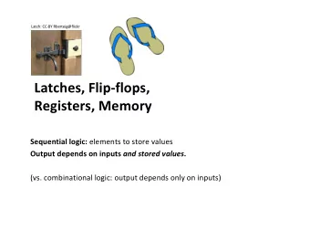
Lecture 7: Sequential Networks CK Cheng Dept. of Computer Science - PowerPoint PPT Presentation
CSE 140: Components and Design Techniques for Digital Systems Lecture 7: Sequential Networks CK Cheng Dept. of Computer Science and Engineering University of California, San Diego 1 Part II: Sequential Networks Introduction
CSE 140: Components and Design Techniques for Digital Systems Lecture 7: Sequential Networks CK Cheng Dept. of Computer Science and Engineering University of California, San Diego 1
Part II: Sequential Networks • Introduction – Sequential circuits – Memory hierarchy – Basic mechanism of memory • Basic Building Blocks – Latches – Flip-Flops – Examples of Memory Modules • Implementation – Finite state machine 2
What is a sequential circuit? “A circuit whose output depends on current inputs and past outputs” “A circuit with memory ” Memory: a key parameter is Time Memory / Time steps s i x i y i Clock 3
Sequential Networks: Key features Memory / Time steps Memory: Flip flops s i x i y i Specification: Finite State Machines Implementation: Excitation Tables Clock Main Theme: Timing Present time = t and next time = t+1 Timing constraints to separate the present and next times. y i = f i (S t ,X) t+1 = g i (S t ,X) s i S t+1 S t Combinational logic X Y clock 4
Sequential Networks: Key features Main Theme: Timing Present time = t and next time = t+1 Timing constraints to separate the present and next times. S t+1 y i = f i (S t ,X) S t Combinational t+1 = g i (S t ,X) s i logic X Y clock S t Combinational logic X Y 5 clock
Different Types of Memory/Storage • Typical Computer Memory Hierarchy • Tradeoff between speed Registers/Latches (latency) and size • Size relates to Register File (Static – Storage density Memory- SRAM) (area/bit) Cache Memory (Static Memory - – Power (power/bit) SRAM) Main Memory (Dynamic Memory – DRAM) NVM Main Memory (Non-Volatile Memory – e.g. Flash) Disk 6
Fundamental Memory Mechanism I1 Q Q Q I2 I1 I2 Q 7
Memory Mechanism: Capacitive Load • Fundamental building block of sequential circuits • Two outputs: Q , Q • There is a feedback loop! • In a typical combinational logic, there is no feedback loop. • No inputs I1 Q Q Q I2 I1 I2 Q 8
Capacitive Loads • Consider the two possible cases: 0 I1 Q – Q = 0: then Q’ = 1 and Q = 0 (consistent) 1 0 1 – Q = 1: then Q ’ = 0 and Q = 1 (consistent) I2 Q – Bistable circuit stores 1 bit of state in the state 1 variable, Q (or Q’ ) I1 Q 0 – Hold the value due to capacitive charges and feedback loop strengthening 1 0 I2 Q • But there are no inputs to control the state 9
iClicker Q. Given a memory component made out of a loop of inverters, the number of inverters in the loop has to be A. Even B. Odd C. No constraints 10
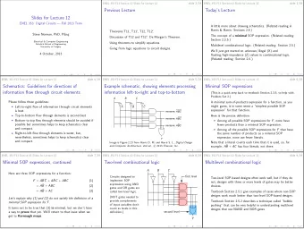
Memory Storage Mechanism • Word line (WL) to access cell WL • Read – measure voltage difference between B+ and B- B+ B- • Write – force values of B+ and B- which may flip the cell • Static Random Sense Amp WriteDriver Access Memory - SRAM 11
Basic Building Blocks • Latches (Level Sensitive) – SR Latches, D Latches • Flip-Flops (Edge Triggered) – D FFs, (JK FFs, T FFs) • Examples of Memory Modules – Registers, Shift Registers, Pattern Recognizers, Counters, FIFOs 12
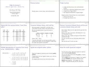
Flight attendant call button • Flight attendant call button – Press call: light turns on Call Blue light button Bit • Stays on after button released Storage Cancel – Press cancel: light turns off button – Logic gate circuit to implement this? 1. Call button pressed – light turns on Call Blue light button Bit • SR latch implementation a Storage Cancel button – Call=1 : sets Q to 1 and keeps it at 1 2. Call button released – light stays on – Cancel=1 : resets Q to 0 Call Blue light C all S button Bit button Storage Cancel button Blue light 3. Cancel button pressed – light turns off Q Cancel button R 13
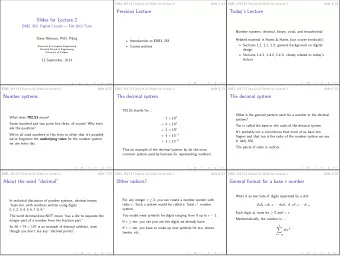
SR (Set/Reset) Latch • SR Latch R N1 Q N2 Q S • Consider the four possible cases: – S = 1, R = 0 – S = 0, R = 1 – S = 0, R = 0 – S = 1, R = 1 14
SR Latch Analysis – S = 1, R = 0: then Q = 1 and Q = 0 0 R N1 Q 1 N2 Q S – S = 0, R = 1: then Q = 0 and Q = 1 1 R N1 Q 0 N2 Q S 15
SR Latch Analysis – S = 0, R = 0: then Q = Q prev Q prev = 0 Q prev = 1 0 0 R 0 R N1 Q N1 Q 0 N2 Q 0 N2 Q S S – S = 1, R = 1: then Q = 0 and Q = 0 1 R N1 Q 1 N2 Q S 16
SR Latch y S y = (S+Q)’ Q Q = (R+y)’ R y S R Q Inputs: S, R State: (Q, y) 17
Truth table of SR latch S R Qt yt Qt yt Qt yt Qt yt id with incremental steps in 0 0 0 0 0 1 1 0 0 1 1 time 1 0 0 0 1 0 1 0 1 0 1 2 0 0 1 0 1 0 1 0 1 0 3 0 0 1 1 0 0 1 1 0 0 y S y = (S+Q)’ 4 0 1 0 0 0 1 0 1 0 1 5 0 1 0 1 0 1 0 1 0 1 6 0 1 1 0 0 0 0 1 0 1 7 0 1 1 1 0 0 0 1 0 1 Q Q = (R+y)’ 1 0 8 1 0 0 0 1 0 1 0 R 9 1 0 0 1 0 0 1 0 1 0 10 1 0 1 0 1 0 1 0 1 0 11 1 0 1 1 0 0 1 0 1 0 12 1 1 0 0 0 0 0 0 0 0 0 0 13 1 1 0 1 0 0 0 0 14 1 1 1 0 0 0 0 0 0 0 18 15 1 1 1 1 0 0 0 0 0 0
S R Qt yt Qt yt Qt yt Qt yt id 0 0 0 0 0 1 1 0 0 1 1 “State Table” of SR latch 1 0 0 0 1 0 1 0 1 0 1 2 0 0 1 0 1 0 1 0 1 0 Qy\SR 00 3 0 0 1 1 0 0 1 1 0 0 01 10 11 4 0 1 0 0 0 1 0 1 0 1 00 11 01 10 00 5 0 1 0 1 0 1 0 1 0 1 0 1 6 0 1 1 0 0 0 0 1 01 01 01 10 00 7 0 1 1 1 0 0 0 1 0 1 8 1 0 0 0 1 0 1 0 1 0 10 10 01 10 00 9 1 0 0 1 0 0 1 0 1 0 11 00 01 10 00 10 1 0 1 0 1 0 1 0 1 0 1 0 11 1 0 1 1 0 0 1 0 12 1 1 0 0 0 0 0 0 0 0 13 1 1 0 1 0 0 0 0 0 0 14 1 1 1 0 0 0 0 0 0 0 19 15 1 1 1 1 0 0 0 0 0 0
CASES: SR=01: (Q,y) = (0,1) SR=10: (Q,y) = (1,0) SR=11: (Q,y) = (0,0) SR= 00: (Q,y) does not change if (Q,y)=(1,0) or (0,1) However, when (Q,y) = (0,0) or (1,1), the output keeps changing Remark: To verify the design, we need to enumerate all combinations. 20
State Table and Q y Q y State Diagram SR State State Next Present Transition State diagram State State 10 00 00 State Table 01 10 01 10 01 10 \SR 00 01 10 11 11 01 Qy 11 00 11 01 10 00 11 00 01 10 01 01 01 10 00 00 00 11 10 10 01 10 00 11 11 00 01 10 00 21
CASES: SR=01: (Q,y) = (0,1) SR=10: (Q,y) = (1,0) SR=11: (Q,y) = (0,0) SR= 00: (Q,y) does not change if (Q,y)=(1,0) or (0,1) However, when (Q,y) = (0,0) or (1,1), the output keeps changing Q . Suppose that we can set the initial state (Q,y)=(0,1). To avoid the SR latch output from toggling or behaving in an undefined way which input combinations should be avoided: A. (S, R) = (0, 0) B. (S, R) = (1, 1) C. None of the above 22
CASES: SR=01: (Q,y) = (0,1) SR=10: (Q,y) = (1,0) SR=11: (Q,y) = (0,0) SR= 00: (Q,y) does not change if (Q,y)=(1,0) or (0,1) However, when (Q,y) = (0,0) or (1,1), the output keeps changing We set the initial state (Q,y)=(0,1) or (1,0). To avoid the state (Q,y)= (0,0) or (1,1), we block the input SR=11. Thus, without input SR=11, the state can only be (Q,y)=(0,1) or (1,0). 23
SR Latch 10 00 00 01 10 01 10 01 10 11 01 11 11 00 01 10 00 00 The only way to reach 11 state (Q,y)=(0,0) or (1,1) is via edge labeled 11 SR=11. 24
SR Latch 10 00 00 01 10 01 10 01 10 11 01 11 11 00 01 10 00 00 The only way to reach 11 state (Q,y)=(0,0) or (1,1) is via edge labeled 11 SR=11. 25
SR Latch Analysis – S = 0, R = 0: then Q = Q prev and Q = Q prev (memory!) Q prev = 0 Q prev = 1 0 0 R 0 R 1 N1 Q N1 Q 1 0 0 1 1 0 0 N2 Q 0 N2 Q S S – S = 1, R = 1: then Q = 0 and Q = 0 (invalid state: Q ≠ NOT Q ) 1 R 0 N1 Q 0 0 0 1 N2 Q S 26
SR Latch CASES SR=01: (Q,y) = (0,1) SR=10: (Q,y) = (1,0) SR=11: (Q,y) = (0,0) SR = 00: if (Q,y) = (0,0) or (1,1), the output keeps changing Solutions: Avoid the case that SR = (1,1). State table SR Characteristic Expression inputs 00 01 10 11 Q(t+1) = S(t)+R’(t)Q(t) PS 0 0 0 1 - Q(t) 1 1 0 1 - Q(t+1) NS (next state) 27
SR Latch Symbol • SR stands for Set/Reset Latch – Stores one bit of state ( Q ) • Control what value is being stored with S , R inputs – Set: Make the output 1 ( S = 1, R = 0, Q = 1 ) – Reset: Make the output 0 ( S = 0, R = 1, Q = 0 ) SR Latch • Must do something to avoid Symbol invalid state (when S = R = 1) R Q S Q 28
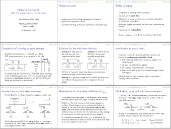
D Latch • Two inputs: CLK , D – CLK : controls when the output changes – D (the data input): controls what the D Latch output changes to Symbol • Function CLK – When CLK = 1, D passes through to Q D Q (the latch is transparent ) – When CLK = 0, Q holds its previous Q value (the latch is opaque ) • Avoids invalid case when Q ≠ NOT Q 29
D Latch Internal Circuit SR Latch Symbol CLK R Q D Q S Q Q 30
D Latch Internal Circuit CLK CLK R R Q Q D D Q S S Q Q D Q CLK D D S R Q Q 0 X 1 0 1 1 31
D Latch Internal Circuit CLK CLK R R Q Q D D Q S S Q Q Q D CLK D D S R Q Q 0 X X 0 0 Q prev Q prev 1 0 1 0 1 0 1 1 1 0 1 0 1 0 32
Recommend
More recommend
Explore More Topics
Stay informed with curated content and fresh updates.


