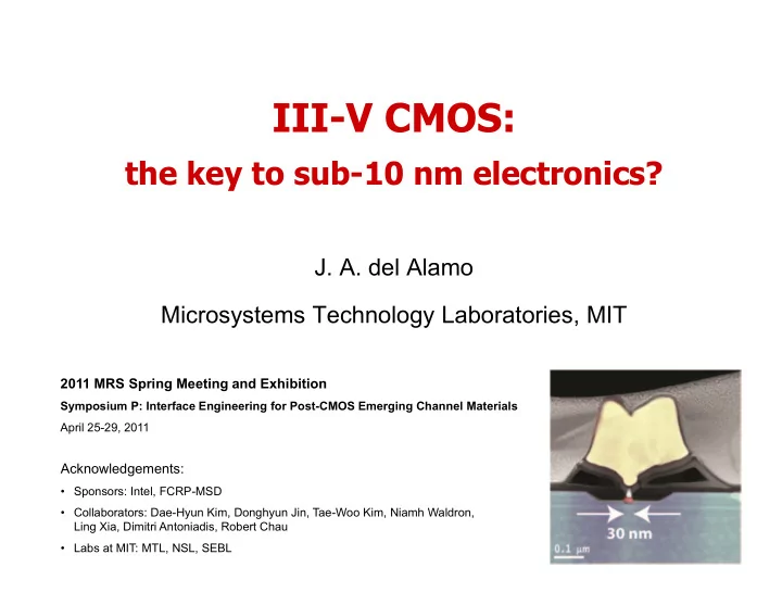
III-V CMOS: the key to sub-10 nm electronics? J. A. del Alamo - PowerPoint PPT Presentation
III-V CMOS: the key to sub-10 nm electronics? J. A. del Alamo Microsystems Technology Laboratories, MIT 2011 MRS Spring Meeting and Exhibition Symposium P: Interface Engineering for Post-CMOS Emerging Channel Materials April 25-29, 2011
III-V CMOS: the key to sub-10 nm electronics? J. A. del Alamo Microsystems Technology Laboratories, MIT 2011 MRS Spring Meeting and Exhibition Symposium P: Interface Engineering for Post-CMOS Emerging Channel Materials April 25-29, 2011 Acknowledgements: • Sponsors: Intel, FCRP-MSD • Collaborators: Dae-Hyun Kim, Donghyun Jin, Tae-Woo Kim, Niamh Waldron, Ling Xia, Dimitri Antoniadis, Robert Chau • Labs at MIT: MTL, NSL, SEBL 1
Outline • Why III-Vs for CMOS? • Lessons from III-V HEMTs • The challenges for III-V CMOS – Critical problems • How will a future 10 nm class III-V FET look like? • Conclusions 2
CMOS scaling in the 21 st century • Si CMOS has entered era of “power-constrained scaling”: – Microprocessor power density saturated at ~100 W/cm 2 – Microprocessor clock speed saturated at ~ 4 GHz Intel microprocessors Pop, Nano Res 2010 3
Consequences of Power Constrained Scaling Power = active power + stand-by power 2 N N ↑ V DD ↓ P A ~ f CV DD clock frequency #1 goal! transistor capacitance operating voltage transistor count Transistor scaling requires reduction in supply voltage Not possible with Si: performance degrades too much 4
How III-Vs allow further V DD reduction? • Goals of scaling: – reduce transistor footprint – extract maximum I ON for given I OFF 5
How III-Vs allow further V DD reduction? • Goals of scaling: – reduce transistor footprint – extract maximum I ON for given I OFF • III-Vs: – higher electron velocity than Si I ON ↑ – tight carrier confinement in quantum well S ↓ sharp turn on 6
InAs High Electron Mobility Transistors Gate S D - QW channel (t ch = 10 nm): Oxide Cap • InAs core (t InAs = 5 nm) Etch stopper Barrier • InGaAs cladding t ins n,Hall = 13,200 cm 2 /V-sec t ch - Channel - InAlAs barrier (t ins = 4 nm) Buffer - Ti/Pt/Au Schottky gate - L g =30 nm Kim, EDL 2010 7 7
L g =30 nm InAs HEMT Kim, EDL 2010 2.0 V GS = 0.4 V 0.8 1.5 0.6 g m [mS/ m] I D [mA/ m] 0.2 V 1.0 0.4 0.5 0.2 0 V V DS = 0.5 V 0.0 0.0 0.0 0.2 0.4 0.6 0.8 -0.6 -0.4 -0.2 0.0 0.2 V DS [V] V GS [V] • Large current drive: I ON >0.5 mA/µm at V DD =0.5 V • V T = -0.15 V, R S =190 ohm. μ m • High transconductance: g mpk = 1.9 mS/ μ m at V DD =0.5 V 8 8 8
L g =30 nm InAs HEMT Kim, EDL 2010 40 3 -3 V DS = 0.5 V 10 H 21 -4 10 30 2 U g f T =644 GHz I D V DS = 0.05 V -5 10 Gains [dB] f max =681 GHz I D , I G [A/ m] MSG/MAG 20 1 -6 10 K V DS = 0.5 V -7 10 10 0 K I G -8 10 V DS =0.5 V, V GS =0.2 V V DS = 0.05 V -9 10 0 -1 -1.0 -0.8 -0.6 -0.4 -0.2 0.0 0.2 0.4 9 10 11 12 10 10 10 10 V GS [V] Frequency [Hz] • FET with highest f T in any material system • Only transistor of any kind with both f T and f max > 640 GHz • S = 74 mV/dec, DIBL = 80 mV/V, I on /I off ~ 5x10 3 • All FOMs at V DD =0.5 V 9 9
InAs HEMTs: Benchmarking with Si • FOM that integrates short-channel effects and transport: I ON @ I OFF =100 nA/µm, V DD =0.5 V Kim EDL 2010 IEDM 2008 (scaled to V DD =0.5 V) InAs HEMTs: higher I ON for same I OFF than Si 10
Why high I ON ? 1. Very high electron injection velocity at the virtual source v inj E C E V Kim, IEDM 2009 Liu, Springer 2010 • v inj (InGaAs) increases with InAs fraction in channel • v inj (InGaAs) > 2v inj (Si) at less than half V DD 11
Why high I ON ? 2. Sharp subthreshold swing due to quantum-well channel state-of-the-art Si 90 In 0.7 Ga 0.3 As HEMTs: t ch = 13 nm Subtreshold swing [mV/dec] 80 InAs HEMTs: t ch = 10 nm 70 InAs HEMTs: t ch = 5 nm t ins = 4 nm, L side = 80 nm Kim, IPRM 2010 60 40 80 120 160 200 L g [nm] • Dramatic improvement in short-channel effects in thin channel devices 12
The Challenges for III-V CMOS: III-V HEMT vs. Si CMOS Intel’s 45 nm CMOS III-V HEMT ~2 m Critical issues: • Schottky gate MOS gate • Footprint scaling [1000x too big!] Need self-aligned design • p-channel device • III-V on Si 13
III-V’s on Si • The challenge: – III-V heterostructures on large-area Si wafers – Thin buffer layer – Low defectivity • Some notable work: XOI InAs MOSFET G S InAs D SiO 2 Si Aspect Ratio Trapping + InAs Nanoribbon Direct III-V MBE on Si Epitaxial Lateral Overgrowth MOSFETs on Insulator (Intel) (Amberwave) (UC Berkeley) Hudait, IEDM 2007 Fiorenza, ECS 2010 Ko, Nature 2010 14
Critical problem: Integration of two different layer structures side-by-side on Si Fiorenza ECS 2010 Key issues: • different lattice constants • planar surface • compact 15
The gate stack • Challenge: metal/high-K oxide gate stack – Fabricated through ex-situ process – Very thin oxide (EOT<1 nm) – Low leakage (I G <10 A/cm 2 ) – Low D it (<10 12 eV -1 .cm -2 in top ~0.3 eV of bandgap) – Reliable • Some notable work: Al 2 O 3 /GGO on InGaAs by TaSiO x on InGaAs by ALD Al 2 O 3 by ALD MBE/ALD (Tsinghua) (Purdue) (Intel) Hong, MRS Bull 2009 Radosavljevic, IEDM 2009 Wu, EDL 2009 16
In 0.7 Ga 0.3 As Quantum-Well MOSFET 2009 Intel InGaAs MOSFET (scaled to V DD =0.5 V) L g =75 nm InGaAs MOSFET outperforms state-or-the-art Si NMOS at 0.5 V Radosavljevic, IEDM 2009 17
Critical problem: Mobility degradation in scaled gate stacks buried channel surface channel Graph courtesy of Prashant Majhi Si (Sematech) reference • μ advantage over Si erodes away in thin barrier structures • Remote Coulomb scattering at oxide/semiconductor interface 18
Self-aligned device architecture • The challenge: – MOSFET structures with scalability to 10 nm – Self-aligned gate design • Some notable work: In-situ Doped S/D for R S Reduction G x In 0.4 Ga 0.6 As y Channel Strain In 0.53 Ga 0.47 As Engineering 60 nm 100 nm for Mobility InP Enhancement Ion-implanted self-aligned Regrown ohmic contact Quantum-well FET with self- InGaAs MOSFET (NUS) MOSFET (NUS) aligned Mo contacts (MIT) Lin, IEDM 2008 Chin, EDL 2009 Kim, IEDM 2010 19
Critical problem: contact scaling Today: ~200 ohm. μ m Need: ~50 ohm. μ m Reduce contact resistivity + resistance of contact stack Waldron, TED 2010 Current contacts to III-V FETs are >100X off in required contact resistance 20
P-channel MOSFETs • The challenge: – Performance >1/3 that of n-MOSFETs – Capable of scaling to <10 nm gate length regime – Co-integration with III-V NMOSFET on Si • Some notable work: Al 2 O 3 by ALD on InGaAs and Ga 2 O 3 /AlGaAs/GaAs Al 2 O 3 /InGaSb QW- MOSFET (Motorola) MOSFET (Stanford) Ge MOSFETs (IMEC) Lin, IEDM 2009 Passlack, EDL 2002 Nainani, IEDM 2010 21
How will a future 10 nm-class III-V MOSFET look like? • Quantum well + raised source/drain + self-aligned gate • Two designs: Recessed gate Regrown source and drain • QW extends under S/D • More freedom for S/D region design high μ preserved • Uniaxial strain possible • Critical interface protected until late in process 22
Critical problem: planar FET might not meet electrostatics requirements • Electrostatic integrity might demand 3D III-V MOSFET structures • Some notable work: Gate Gate Source Source Drain Drain Fin-Channel Fin-Channel Fin-Channel Fin-Channel Fin-Channel Fin-Channel EXT. EXT. Fin-channel Fin-channel p InP p InP p+ InP p+ InP InAs Vertical Nanowire InAs Nanowire FETs InGaAs FinFET (Purdue, Intel) (UC Berkeley) FETs (Lund) Wu, IEDM 2009 Egard, NanoLett 2010 Chueh, NanoLett 2008 Radosavljevic, IEDM 2010 23
Conclusions • III-Vs attractive for CMOS: key for low V DD operation – Electron injection velocity > 2X that of Si at 1/2X V DD – Quantum-well channel yields outstanding short-channel effects • Impressive recent progress on III-V CMOS – Ex-situ ALD and MOCVD on InGaAs yield interfaces with unpinned Fermi level and low defect density – Sub-100 nm InGaAs MOSFETs with I ON > than Si at 0.5 V demonstrated • Lots of work ahead – Demonstrate 10 nm III-V N-MOSFET that is better than Si – P-channel MOSFET – N-channel + P-channel cointegration 24
Recommend
More recommend
Explore More Topics
Stay informed with curated content and fresh updates.
