Development of a Concurrent Dual-Band Switch-Mode Power Amplifier - PowerPoint PPT Presentation
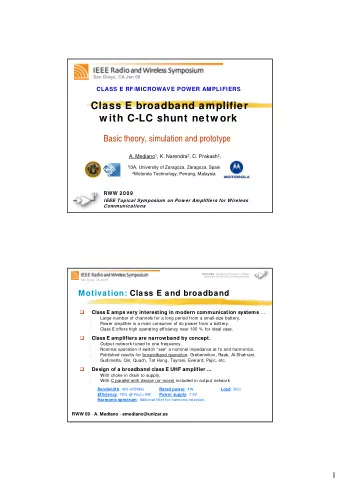
Development of a Concurrent Dual-Band Switch-Mode Power Amplifier Based on Current- Switching Class-D Configuration Yifei Li, Byron J. Montgomery and Nathan M. Neihart Iowa State University WAMICON 2016 Clearwater Beach, FL Contents
Development of a Concurrent Dual-Band Switch-Mode Power Amplifier Based on Current- Switching Class-D Configuration Yifei Li, Byron J. Montgomery and Nathan M. Neihart Iowa State University WAMICON 2016 – Clearwater Beach, FL
Contents Contents Background and Motivation Theoretical Analysis of Proposed Concurrent Dual- band Class-D Power Amplifier Design Method and Considerations Measurement Results and Discussion 2
Demand for Concurrent Multi-Band PAs Demand for Concurrent Multi-Band PAs Higher data rate (carrier aggregation) By using concurrent (multi-)dual-band PAs, we are trying to reduce area, cost, design complexity and increase efficiency as well. f 1,dn f 1 f 1,up PA 1 f 1 ,f 2 Improve Duplexer f 1 ,f 2 f 1 ,f 2 Duplexer Dual-Band f 2,up Concurrent Diplexer PA 2 Duplexer Dual-Band f 1 ,f 2 f 2 PA Single- f 2,dn Band PA Proposed TX Schematic for CA Currently Used TX Schematic for CA 3
Existing Concurrent Dual-Band PAs Existing Concurrent Dual-Band PAs Linear PAs are used to accommodate the varying envelope of concurrent dual-band signals Theoretical Maximum Drain efficiency of Linear PAs 2 ∗ 𝑊 ∗ 𝐽 𝑒𝑡,𝑛𝑏𝑦 2 ∗ 1 𝑒𝑡,𝑛𝑏𝑦 η = 𝑄 = 𝑄 𝑝1 + 𝑄 2𝜷 2𝜷 𝑝 𝑝2 Concurrent Dual-Band Class A = 𝑒𝑡,𝑛𝑏𝑦 /2 ∗ 𝐽 𝑒𝑡,𝑛𝑏𝑦 /2 = 25% 𝑄 𝑊 𝐸𝐸 ∗ 𝐽 𝐸𝐷 𝑊 𝐸𝐷 2 ∗ 𝑊 ∗ 𝐽 𝑒𝑡,𝑛𝑏𝑦 2 ∗ 1 𝑒𝑡,𝑛𝑏𝑦 η = 𝑄 = 𝑄 𝑝1 + 𝑄 2𝜷 𝜸 𝑝 𝑝2 = 𝑒𝑡,𝑛𝑏𝑦 /2 ∗ 𝐽 𝑒𝑡,𝑛𝑏𝑦 /𝜹 = 62% Concurrent Dual-Band Class B 𝑄 𝑊 𝐸𝐸 ∗ 𝐽 𝐸𝐷 𝑊 𝐸𝐷 Note: 𝛽, 𝛾, 𝛿 are about 2, 4, and 5 respectively in most cases (non-harmonic related frequency ratio). V ds V ds 2 2 + I ds I ds 1.5 1.5 V ds and I ds V ds and I ds 1 1 0.5 0.5 0 0 0 0.5 1 1.5 2 0 0.5 1 1.5 2 Time Time Concurrent Dual-Band Class B Concurrent Dual-Band Class A Input Waveform Z. Zhang, MWCAS, 2015. 4 X. Chen, MTT 2013
Existing Concurrent Dual-Band PAs in Literatures Switchless Dual-Band PA: IMs not considered Pout @ Efficiency @ Frequency Pout @ Single Efficiency @ Concurrent Concurrent Signal (GHz) Mode Single Mode Mode Mode IET MAP, 2011 1.96/3.5 39.5/40 dBm 39.5 dBm 60%/55% 49% CW WAMICON, 2012 1.8/2.4 35.5/35.5 dBm 33 dBm 34.7%/32.7% 24.7% WCDMA/LTE T-MTT, 2012 1.8/2.4 36.2/34.5 dBm 33.4 dBm 54.2%/40.7% 34.4% LTE/WiMax TCAS I, 2014 0.85/2.33 44/42.5 dBm 31.4 dBm 60%/53% 26.7% CW/LTE Linear Concurrent Dual-Band PAs: IMs shorting Frequency Pout @ Single Pout @ Efficiency @ Efficiency @ Signal (GHz) Mode Concurrent Mode Single Mode Concurrent Mode T-MTT, 2012 1.9/2.6 41.5/41.2 dBm 39.5 dBm 73%/67.5% 56% CW IMS, 2014 1.9/2.6 44.5/44 dBm 42 dBm 65%/60% 53% CW Switch-Mode Concurrent Dual-Band PAs? Higher concurrent-mode output power Higher concurrent-mode efficiency 5
Contents Contents Backgrounds and Motivations Theoretical Analysis of Proposed Concurrent Dual- band Class-D Power Amplifier Design Method and Considerations Measurement Results and Discussion Conclusion 6
Proposed Concurrent Dual-Band Current- Proposed Concurrent Dual-Band Current- Switching Class-D PA Switching Class-D PA M1 + I DSP 3 V IP V DSP + V IM 2 * * V IP I DC Magnitude [V] - - + I O 1 * * V B + R L + * - Dual-Band V O 0 V in * VDD Shunt - - V IM - -1 Resonator - + V DSM XMR_out XMR_in -2 I DSM M2 + 0 0.5 1 1.5 2 Time Idealized analysis: zero knee voltage, zero threshold voltage Input signal Harmonic related frequencies, 𝑊 𝐽𝑄 𝑢 = 𝐵 𝑡𝑗𝑜 𝜕 1 𝑢 + 𝐵 𝑡𝑗𝑜 𝜕 2 𝑢 + 𝑊 𝐶 𝝏 𝟑 /𝝏 𝟐 =2, 3, are avoided. 𝑊 𝐽𝑁 𝑢 = 𝐵 𝑡𝑗𝑜 𝜕 1 𝑢 + 𝜌 + 𝐵 𝑡𝑗𝑜 𝜕 2 𝑢 + 𝜌 + 𝑊 𝐶 7
Transistor transfer function I DSP(M) I DC 0, 𝑊 𝑢 < 𝑊 𝑢ℎ = 0 𝐽𝑄 𝑁 𝐽 𝐸𝐷 𝐽 𝐸𝑇𝑄 𝑁 𝑢 = 𝑊 𝑢 , 𝑊 𝑢ℎ < 𝑊 𝑢 < 2𝑊 𝐽𝑄 𝑁 𝐽𝑄 𝑁 𝐶 2𝑊 I DC /2 𝐶 𝐽 𝐸𝐷 , 𝑊 𝑢 > 2𝑊 𝐽𝑄 𝑁 𝐶 V IP (V IM ) V th =0 V B 2V B Assuming the PA is overdriven, I DC is fixed Determined by V DD and R L , independent of A I DC can be accommodated by changing V DD or R L when 𝑊 𝐶 changes Drain Current and Output Current 𝐽 0 = 𝐽 𝐸𝑇𝑄 − 𝐽 𝐸𝑇𝑁 𝑂 𝑁 𝐽 𝑝 𝑢 ≈ 𝐽 𝑛,𝑜 ∗ sin ( 𝑛𝜕 1 ± 𝑜𝜕 2 𝑢 + 𝜄 𝑛,𝑜 ) 𝑜=0 𝑛=0 Where 𝐽 0,0 , 𝐽 0,1 , 𝐽 1,0 represent DC and two fundamentals respectively. 8
M1 + I DSP Transistor transfer function V DSP + * * V IP I DC I DSP(M) I DC - 0, 𝑊 - 𝑢 < 𝑊 𝑢ℎ = 0 + I O 𝐽𝑄 𝑁 * * V B 𝐽 𝐸𝐷 + R L + * - Dual-Band V O 𝐽 𝐸𝑇𝑄 𝑁 𝑢 = 𝑊 𝑢 , 𝑊 𝑢ℎ < 𝑊 𝑢 < 2𝑊 𝐽𝑄 𝑁 𝐽𝑄 𝑁 𝐶 V in * 2𝑊 I DC /2 VDD 𝐶 Shunt - - V IM 𝐽 𝐸𝐷 , 𝑊 𝑢 > 2𝑊 - 𝐽𝑄 𝑁 𝐶 Resonator - + V DSM XMR_out V IP (V IM ) XMR_in I DSM M2 + V th =0 V B 2V B Assuming the PA is overdriven, I DC is fixed Determined by V DD and R L , independent of A I DC can be accommodated by changing V DD or R L when 𝑊 𝐶 changes Drain Current and Output Current 𝐽 0 = 𝐽 𝐸𝑇𝑄 − 𝐽 𝐸𝑇𝑁 𝑂 𝑁 𝐽 𝑝 𝑢 ≈ 𝐽 𝑛,𝑜 ∗ sin ( 𝑛𝜕 1 ± 𝑜𝜕 2 𝑢 + 𝜄 𝑛,𝑜 ) 𝑜=0 𝑛=0 Where 𝐽 0,0 , 𝐽 0,1 , 𝐽 1,0 represent DC and two fundamentals respectively. 9
Output Voltage and Drain Voltage V DSP 1.2 V o t = R L I 1,0 sin ω 1 t + θ (1,0) + I 0,1 sin ω 2 t + θ (0,1) I DSP 1 Magnitude 𝑊 𝐸𝑇𝑄(𝑁) 𝑢 = 0.5 𝑊 𝑝 𝑢 ± 𝑊 𝑝 𝑢 A/V B =5 0.8 A/V B =2 A/V B =1 0.6 A/V B =5 Drain Efficiency A/V B =2 0.4 A/V B =1 𝑈 0.2 𝐸𝐸 = 1 𝑊 𝑈 0.5 𝑊 𝐸𝑇𝑄 𝑢 + 𝑊 𝐸𝑇𝑁 (𝑢) 𝑒𝑢 0 0 0 0.5 1 1.5 2 Time 2 2 (I (0,1) +I (1,0) )𝑆 𝑀 𝜃 = 𝑄 𝑆𝐺 = 100 20 20 20 𝑄 2 𝑊 𝐸𝐸 𝐽 𝐸𝐷 𝐸𝐷 Drain Efficiency Drop(%) Drain Efficiency(%) 90 15 15 15 What will happen with non-zero knee voltage? A/V B =1 80 10 10 10 A/V B =2 A/V B =5 70 5 5 5 60 0 0 0 1 1 1 1 2 2 2 2 3 3 3 3 4 4 4 4 2 / 1 10
Non-Zero Knee Voltage Non-Zero Knee Voltage I DC V B Bias Saturation Triode Bias V B 245mA 176mA current 464mA 468mA I DC V DC 15V 15V I Bias R L 50Ω 40Ω XMR 2:1 2:1 ratio 𝜽 93.4% 77.5% 11
Contents Contents Backgrounds and Motivations Theoretical Analysis of Proposed Concurrent Dual- band Class-D Power Amplifier Design Method and Considerations Measurement Results and Discussion Conclusion 12
Design Method Design Method Ideal transformer and shunt resonator provides: Z Load = Ideal open @ even harmonics and IMs Z Load = Ideal short @ odd harmonics and IMs Z Load = R opt @ fundamentals Order of Frequency I DSP (A) V DSP (V) * Nonlinearity + * Z Load R L * Dual-Band DC 0 0.5 0.155 Shunt 𝝏 𝟐(𝟑) 1 0.38 0.19 Resonator - XMR_out 𝝏 𝟑 ± 𝝏 𝟐 2 0 0.1 2 𝝏 𝟐(𝟑) 2 0 0.04 Ideal Load Network 𝟑𝝏 𝟐(𝟑) − 𝝏 𝟑(𝟐) 3 0.09 0 𝟑𝝏 𝟐(𝟑) + 𝝏 𝟑(𝟐) 3 0.1 0 3 𝝏 𝟐 3 0.02* 0 3 𝝏 𝟑 3 0.008* 0 13
Implementation Considerations Implementation Considerations Output network target: Z opt @ fundamentals; high impedance @ even-order harmonic and IM (especially 2 nd -order); low impedance @ odd-order harmonic and IM C out Differential: absorbed in to dual-band shunt resonator Common-mode: needs to be resonated out by the output network Output Matching V in V B f 1 V DD Distributed Output 50 Ω Marchand Input Matching f 2 Balun Matching Output Input Balun Network 14
Board Layout Board Layout V DD Output Balun V B Output Matching Differential Input Shunt Resonator Input Balun Matching V B V DD 15
Contents Contents Backgrounds and Motivations Theoretical Analysis of Proposed Concurrent Dual- band Class-D Power Amplifier Design Method and Considerations Measurement Results and Discussion Conclusion 16
Measurement Results Measurement Results Single Mode Low band: 𝜃 = 55.6% @ Pout=30dBm; 6dB over drive High band: 𝜃 = 48.2% @ Pout=30dBm; 6dB over drive Concurrent Dual-Band Mode 𝜃 = 46% @ Pout=29.7dBm; 6dB over drive 60 18 18 18 30 50 15 15 15 Output Power(dBm) Drain Efficiency(%) Power Gain(dB) 40 12 12 12 26 Single Mode@960MHz 30 9 9 9 Single Mode@1.51GHz Single Mode@960MHz 22 Concurrent Mode Single Mode@1.51GHz 20 6 6 6 Concurrent Mode Concurrent Mode @960MHz 10 3 3 3 18 Concurrent Mode @1.51GHz 0 0 0 0 0 5 10 15 20 25 20 20 20 20 22 22 22 22 24 24 24 24 26 26 26 26 28 28 28 28 30 30 30 30 17 Input Power(dBm) Output Power(dBm)
Recommend
More recommend
Explore More Topics
Stay informed with curated content and fresh updates.

![1 [9-4] Mor M. Peretz, Switch-Mode Power Supplies Current feedback loop I o L i o V o v o S V](https://c.sambuz.com/1071065/1-s.webp)

![1 Mor M. Peretz, Switch-Mode Power Supplies [8-4] Control of PWM converters disturbances in](https://c.sambuz.com/1062650/1-s.webp)
![1 [2-4] Mor M. Peretz, Switch-Mode Power Supplies Capacitor types Polarized (electrolytic) Non](https://c.sambuz.com/1065911/1-s.webp)
