An Interconnect-Centric Design Flow for Nanometer Technologies - PDF document
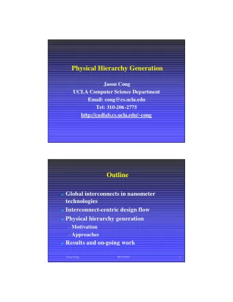
An Interconnect-Centric Design Flow for Nanometer Technologies Professor Jason Cong Professor Jason Cong <cong cong@cs.ucla. @cs.ucla.edu edu> UCLA Computer Science Department UCLA Computer Science Department Los Angeles, CA 90095
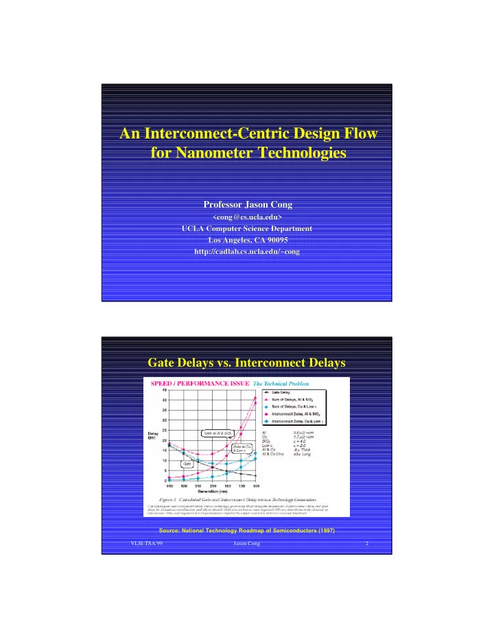
An Interconnect-Centric Design Flow for Nanometer Technologies Professor Jason Cong Professor Jason Cong <cong cong@cs.ucla. @cs.ucla.edu edu> UCLA Computer Science Department UCLA Computer Science Department Los Angeles, CA 90095 Los Angeles, CA 90095 http:// http://cadlab cadlab.cs cs.ucla ucla.edu edu/~ /~cong cong Gate Delays vs. Interconnect Delays Source: National Technology Roadmap of Semiconductors (1997) VLSI-TSA'99 Jason Cong 2
Interconnect-Centric Design Methodology I Proposed transition Proposed transition interconnect device device interconnect device/function centric interconnect/communication centric I Analogy Analogy Data/Objects Programs Programs Data/Objects VLSI-TSA'99 Jason Cong 3 Interconnect-Centric Design Flow I Key steps in an interconnect Key steps in an interconnect-centric design flow: centric design flow: N Interconnect Planning Interconnect Planning N Interconnect Synthesis Interconnect Synthesis N Interconnect Layout Interconnect Layout I Other supporting tools to enable an interconnect Other supporting tools to enable an interconnect- centric design flow centric design flow N Interconnect performance estimation Interconnect performance estimation N Interconnect performance verification Interconnect performance verification VLSI-TSA'99 Jason Cong 4
Outline of the Talk I Interconnect Synthesis Interconnect Synthesis I Interconnect Performance Estimation Interconnect Performance Estimation I Interconnect Planning Interconnect Planning VLSI-TSA'99 Jason Cong 5 Interconnect Synthesis Optimized interconnect designs: Constraints: Topology • Delay Sizing • Skew • Signal integrity Buffer insertion ... Spacing I Automatic solutions guided by accurate interconnect Automatic solutions guided by accurate interconnect models models VLSI-TSA'99 Jason Cong 6
Example: Single-Net Optimal Wire Sizing (OWS) [Cong-Leung, ICCAD’93] I Given: Given: A set of possible wire widths { W A set of possible wire widths { W 1 , W , W 2 , …, , …, W r } I Find: Find: An optimal wire width assignment to minimize An optimal wire width assignment to minimize distributed RC delay distributed RC delay Wiresizing Optimization Example: Global Interconnect Sizing and Spacing (GISS) [Cong et al, ICCAD’97] Sizing Spacing I Given: Given: N Initial layout of multiple nets Initial layout of multiple nets N Critical sinks and their Critical sinks and their criticalities criticalities N Capacitance model and design rules Capacitance model and design rules I Output: Output: N Sizing and spacing of every net to minimize RC Sizing and spacing of every net to minimize RC delays with consideration of coupling cap. delays with consideration of coupling cap. VLSI-TSA'99 Jason Cong 8
Capacitance Model C x c f Ca I 2.5D capacitance model 2.5D capacitance model [Cong Cong et al, DAC’97] et al, DAC’97] N Consider: C Consider: C a (area), (area), C f (fringing) and (fringing) and C x (coupling) (coupling) N Build capacitance table from 3D field solver ( Build capacitance table from 3D field solver (FastCap FastCap) N Table lookup by interpolation and extrapolation Table lookup by interpolation and extrapolation Main Approaches to GISS I Heuristic: Optimize one net at a time: bottom Heuristic: Optimize one net at a time: bottom- up dynamic programming (optimal for one net) up dynamic programming (optimal for one net) I Better approach: Compute upper and lower Better approach: Compute upper and lower bounds of opt. wire widths/spacings bounds of opt. wire widths/ spacings of all nets of all nets N Extended local refinement (ELR) using generalized Extended local refinement (ELR) using generalized CH CH-posynomial posynomial formulation formulation N Or iterative bound refinement (BR) Or iterative bound refinement (BR) N In practice, lower and upper bounds meet most of In practice, lower and upper bounds meet most of time => optimal solution. time => optimal solution. VLSI-TSA'99 Jason Cong 10
GISS Optimization Results I 16 16-bit 10mm bus structure equally spaced, with 5 bit 10mm bus structure equally spaced, with 5 different center different centerspacings spacings from 2x to 5x min. pitch from 2x to 5x min. pitch I pitch = min. width + min.spacing pitch = min. width + min.spacing Center spacing Average Delays(ns) MIN OWS GISS/S GISS/M 2 x pitch 1.51 1.26 (-17%) 0.82 (-46%) 0.76 (-50%) 3 x pitch 1.33 0.73 (-45%) 0.56 (-58%) 0.50 (-62%) 4 x pitch 1.28 0.46 (-64%) 0.45 (-65%) 0.40 (-69%) 5 x pitch 1.25 0.38 (-70%) 0.37 (-70%) 0.35 (-72%) I For non For non-equal net weights, GISS/M shall have more equal net weights, GISS/M shall have more advantage than GISS/S advantage than GISS/S VLSI-TSA'99 Jason Cong 11 UCLA TRIO Package (Tree, Repeater, Interconnect Optimization) I Synthesis/optimization capabilities Synthesis/optimization capabilities N Interconnect topology optimization Interconnect topology optimization N Optimal buffer insertion Optimal buffer insertion N Wiresizing Wiresizing optimization optimization N Global interconnect sizing and spacing Global interconnect sizing and spacing N Simultaneous driver, buffer, and interconnect sizing Simultaneous driver, buffer, and interconnect sizing N Simultaneous topology generation with buffer insertion and Simultaneous topology generation with buffer insertion and wiresizing wiresizing N ... ... I Efficient polynomial Efficient polynomial-time optimal/near time optimal/near-optimal algorithms optimal algorithms I Interconnect performance can be improved by up to 7x ! Interconnect performance can be improved by up to 7x ! I Available on the web: Available on the web: http:// http://cadlab cadlab.cs cs.ucla ucla.edu edu/~trio /~trio Demo at DAC’99 Demo at DAC’99 VLSI-TSA'99 Jason Cong 12
Impact of Interconnect Optimization -- For a 2cm Global Interconnect Using the TRIO Package 5 2cm DS 4.5 4 2cm BIS 3.5 Delay (ns) 2cm BISWS 3 2.5 G DS: Driver Sizing only 2 G BIS: Buffer Insertion 1.5 and Sizing 1 G BISWS: Simultaneous 0.5 Buffer Insertion/Sizing 0 and Wiresizing 0.25 0.18 0.15 0.13 0.1 0.07 Technology ( u m) 5x ~ 7x performance improvement! Interconnect Synthesis in Layout Design Flow Chip-planning, Floorplaning, Global Int. Planning and Optimization Topology Topology Optimization Optimization Timing Driven Placement Buffer Buffer Delay Budgeting Insertion Insertion Device Sizing Device Sizing Performance Driven Global Wiresizing Routing Wiresizing . . . . . with Interconnect Optimization . . . . . Interconnect Detailed Routing Optimizations with Variable Width and Spacing Library (e.g. TRIO) VLSI-TSA'99 Jason Cong 14
Outline of the Talk I Interconnect Synthesis Interconnect Synthesis I Interconnect Performance Estimation Interconnect Performance Estimation I Interconnect Planning Interconnect Planning VLSI-TSA'99 Jason Cong 15 Interconnect Performance Estimation C s1 G S 1 G 0 S n C sn Input S 2 C s2 I Problem: Estimate the optimized interconnect Problem: Estimate the optimized interconnect delay, area, etc., without actually running the delay, area, etc., without actually running the optimization algorithms (such as TRIO)! optimization algorithms (such as TRIO)!
Needs for Interconnect Performance Estimation Models I Efficiency Efficiency N need to explore many micro need to explore many micro-architectures/ architectures/floorplans floorplans => require to process > 1 million nets/second => require to process > 1 million nets/second N cannot afford actual synthesis/optimization (1 cannot afford actual synthesis/optimization (1-100 nets/second) 100 nets/second) I Abstraction Abstractionto hide detailed design information to hide detailed design information N granularity of wire segmentation granularity of wire segmentation N number of wire widths, buffer sizes, ... number of wire widths, buffer sizes, ... I Explicit relation Explicit relationto enable optimal design decision at high to enable optimal design decision at high levels levels I Result: Result: very efficient (constant very efficient (constant-time) estimation models time) estimation models for various interconnect optimization operations for various interconnect optimization operations Example: Delay/Area Estimation under OWS I Closed Closed-form form delay estimation formula delay estimation formula α α l 2 l 1 1 = + + ⋅ T ( R , l , C ) R c R rc c l l + ows d L d f d a f α α 2 W ( l ) W ( l ) 2 2 where rc α α 1 1 a rc , 2 = 1 = a 2 R C 4 d L w = W(x) is Lambert’s W function defined as we x I Closed Closed-form form area estimation formula area estimation formula + r ( c l 2 C ) = ⋅ f L A ( R , l , C ) l ows d L 2 R c d a
Recommend
More recommend
Explore More Topics
Stay informed with curated content and fresh updates.

