RF-Interconnect RF-Interconnect and its Applications to and its - PDF document
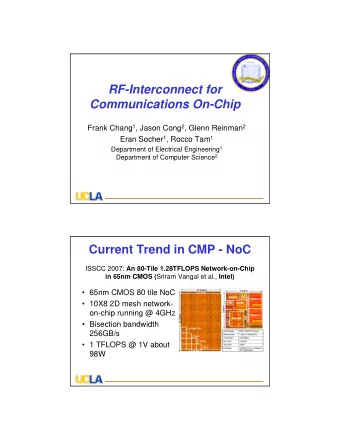
RF-Interconnect RF-Interconnect and its Applications to and its Applications to NoC Design NoC Design NOCS Tutorial Course, NOC Tutorial Course, May 10 2009 y 10 2009 San Diego, California San Diego, Californ Frank Chang, Jason Cong and
RF-Interconnect RF-Interconnect and its Applications to and its Applications to NoC Design NoC Design NOCS Tutorial Course, NOC Tutorial Course, May 10 2009 y 10 2009 San Diego, California San Diego, Californ Frank Chang, Jason Cong and Glenn Reinman E-mails: mfchang@ee.ucla.edu cong@cs.ucla.edu Glenn.reinman@cs.ucla.edu 1 RF-Interconnect RF-Interconnect 2 1
Outline • Future Network-on-Chip (NoC) needs and development trends • Traditional baseband-interconnect constraints • Multiband RF-Interconnect (RF-I) advantages – Scalability in latency, energy/bit, data rate (Gbps/link) and overhead (area/Gb) – On-chip demonstrations – Off-chip demonstrations – Remaining technology challenges • Potential RF-I system applications 3 Current Trend in CMP ISSCC 2007: An 80-Tile 1.28TFLOPS Network-on-Chip in 65nm CMOS ( Sriram Vangal et al., Intel) • 65nm CMOS 80 tile NoC • 10X8 2D mesh network-on- chip running @ 4GHz • Bisection bandwidth 256GB/s • 1 TFLOPS @ 1V about 98W • Needs total 75 Clk cycles from the lower left corner to the upper right corner 4 2
Future CMP Development Trends: • Heterogeneous/domain-specific system architecture • Many-core massive parallel data processing • System integration in deep-scaled CMOS technology • Low supply voltage with sub-V th digital operation Issues: • Performance increasingly dependent on inter-core or inter-system communications 5 Scaling of Traditional Interconnect f T 10 • Scaling reduces delay of logic gates but not of wires • Latency is RC limited (~L 2 ) • Using CMOS repeaters reduces latency (~L) but receives no benefit from scaling • Even low swing signaling requires extensive equalization • Waste of broad bandwidth available from modern CMOS devices (f t >150GHz, f max >250GHz) 6 3
Baseband Interconnect Issues • Latency is large across the chip • Bandwidth is RC limited (~1Gbps/wire) • Communication pattern is fixed (non-reconfigurable) • Energy consumption is high and not scalable (~10pJ/bit/cm) • At 22nm technology, the total network power using buffer can be as high as 150W* • Future microprocessors may encounter communication congestion and most of the energy will be spent on “talking” instead of computing *“Research Challenges for On-Chip Interconnection Networks,” IEEE Micro, 2007 7 Communication Challenges • On-Chip Issues – # Cores in Chip-Multiprocessor (CMP) growing • Increasing bandwidth demand on interconnect – Wires scaling poorly compared to transistors • Increased latency to communicate between distant points on CMP • Off-chip limited by chip-to-chip, board-to-board, board-to-backplane communications • Requirements on future interconnect – Scalable, reliable – Support high traffic volume with low latency – Constrained by • Power • Silicon Area • Cost (compatibility with mainstream CMOS technology) 8 4
How Can RF Help? • f T will exceed 600GHz at16nm and f max will even approach 1THz! • Millimeter-wave CMOS circuits have been developed for 60GHz and recently for 324 GHz bands* • Incredible bandwidth is available in future but most people neglect that! • EM waves travel at the (effective) speed of light (~7ps/mm in Silicon) * Huang, Larocca and Chang, “324GHz CMOS Frequency Generator using Linear Superposition Technique,” pp. 476- 477, 2008 ISSCC 9 UCLA 90nm CMOS VCO at 324GHz (ISSCC 2008*) -70 323.5GHz VCO -80 Pout (dBm) CMOS VCO designed by Frank -90 Chang’s group at UCLA, fabricated in 90nm process -100 323.038 323.238 323.438 323.638 323.838 324.0 Frequency (GHz) CMOS Voltage Controlled Oscillator, measured with a subharmonic mixer and driven with a 80 GHz synthesizer local oscillator. The mixing frequency is ( f VCO - 4* f LO )= f IF , or f VCO -4*(80 GHz)= 3.5 GHz, yielding f VCO = 323.5 GHz! On-Wafer VCO Test Setup at JPL *Huang, D., LaRocca T., Chang, M.-C. F., “324GHz CMOS Frequency Generator Using Linear Superposition Technique IEEE International Solid-State Circuits Conference (ISSCC), 476-477, (Feb 2008) San Francisco, CA 10 5
4xf 0 by Linear Superposition 4xfo by Linear Superposition 11 Communication beyond Baseband • Ultra-high carrier frequencies can be generated and modulated by modern CMOS to enable simultaneous multiband communications with higher aggregate data rate • On/off-chip Transmission lines and off- chip near-field antennas can guide waves (RF modulated data) from transmitter to receiver with recoverable attenuation in short distances (<30cm) 12 6
Multiband Communications • Carrier frequencies can be generated and modulated using modern CMOS to enable simultaneous multiband communications with higher aggregate data rate • Higher carrier frequencies can avoid baseband digital noise and cause less frequency dispersion across the band 13 RF-Interconnect Concept Advantages: • Higher combined data rate • Simultaneous, bi-directional communications • Re-configurable between bands f 0 • Low in-band coupling for parallel bus • Potentially with fewer I/O pins and smaller routing Bi-directional Bus area 14 7
Differential Transmission Line • Loss of 1.5dB/mm over 100GHz of Bandwidth Differential TL: 3um 3um IBM 90nm Process 3um Width: 3um 0.5um M8 Spacing: 3um 0.5um M7 Total Thickness: Two Top Metal = 1µm Metal Resistivity: 0.0424Ohm/Sq 15 Multiband FDMA-Interconnect Signal Power Signal Power Signal Power Signal Power Signal Spectrum • In TX, each mixer up-converts individual baseband streams into specific frequency band (or channel) • N different data streams (N=6 in exemplary figure above) may transmit simultaneously on the shared transmission medium to achieve higher aggregate data rates • In RX, individual signals are down-converted by mixer, and recovered after low-pass filter 16 8
FDMA-Interconnect System a 0 t a D Data 1 D a t a N - 2 power 17 Incredible CMOS Bandwidth 1000 Technology (nm) 90 65 45 32 22 16 ft_DRAM 900 fmax_DRAM Number of Cores 8 16 40 64 120 189 800 ft_NFET BW (Bisection) 700 fmax_NFET [GB/s] 91 128 202 256 350 440 freq (G H z ) 600 Chip Power (total) [W] 100 120 144 173 207 249 500 400 fmax [GHz] 200 270 370 480 590 710 300 fvco [GHz] 320 432 592 768 944 1136 200 Max Aggregate Data Rate 100 [Gb/s/wire] 160 216 296 384 472 568 20 30 40 50 60 70 channel length (nm) Maximum aggregate data rate for RF-Interconnect can reach 500Gb/s/wire @16nm Tech Node 18 9
Advantages of RF-I over Parallel Bus • Latency – speed-of-light data transmission • Bandwidth – high aggregate data rate through simultaneous transmissions on multiple bands of RF modulated signals • Area – avoid extensive use of repeaters • Energy – low overall energy bit • Reconfigurability – efficient bidirectional and tunable communications via shared on/off-chip transmission lines or off-chip antennas 19 RF-Interconnect Demonstrations • Off-chip (On-board) Simultaneous Dual- band Communications through RF- Interconnect (ISSCC 05) • Inter-layer 3DIC RF-Interconnect (ISSCC 07) • On-chip Simultaneous generation of multi- band carriers (RFIC 08) • On-Chip Tri-band simultaneous communications (VLSI 09) 20 10
Off-Chip FDMA Links (ISSCC 05*) • 2 carrier RF-I provide simultaneous off chip between 4 CMOS chip in 0.18um technology • 1 baseband and 1 RF band at 7.4GHz • Selectivity between bands is achieved using bandpass or lowpass filtering. • The RF carrier was modulated using BPSK. • Using this scheme, simultaneous data rates of *J. Ko, J. Kim, Z. Xu, Q. Gu, C. Chien, and M.F. Chang, “An (2+2) Gb/s were achieved in RF/Baseband FDMA-Interconnect Transceiver for Reconfigurable Multiple Access Chip-to-Chip Communication,” in 2005 IEEE both the baseband (2Gbps) International Solid-State Circuits Conference (ISSCC) Digest of and the RF band (2Gbps). Technical Papers , February 2005 21 3D-IC Layer-to-Layer RF- Interconnect (ISSCC 07*) • 3DIC RF-I in MIT- Lincoln Lab 0.18 μ m 3DIC technology • Data is modulated with amplitude shift keying (ASK) modulation of a 25GHz carrier • low energy-per-bit: 0.39pJ/bit (a) Schematic of 3DIC RF-I (b) Eye • high data rate: 11Gb/s diagram with 11Gb/s data rate (c) Die photo of the 3DIC RF-I • Q. Gu, Z. Xu, J. Ko and M.F. Chang, "Two 10Gbps/pin Low Power Interconnect Methods for 3D IC", 2007 IEEE International Solid-State Circuits Conference (ISSCC) Digest of Technical Papers , vol.50, pp.448-449, Feb. 2007, San Francisco, California, USA 22 22 11
Recommend
More recommend
Explore More Topics
Stay informed with curated content and fresh updates.





![CS184c: Computer Architecture [Parallel and Multithreaded] Day 15: May 29, 2001 Interconnect](https://c.sambuz.com/865006/cs184c-computer-architecture-parallel-and-multithreaded-s.webp)
