RF-Interconnect for Communications On-Chip Frank Chang 1 , Jason - PDF document
RF-Interconnect for Communications On-Chip Frank Chang 1 , Jason Cong 2 , Glenn Reinman 2 Eran Socher 1 , Rocco Tam 1 Department of Electrical Engineering 1 Department of Computer Science 2 Current Trend in CMP - NoC ISSCC 2007: An 80-Tile
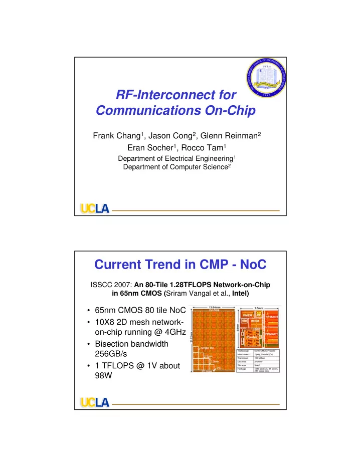
RF-Interconnect for Communications On-Chip Frank Chang 1 , Jason Cong 2 , Glenn Reinman 2 Eran Socher 1 , Rocco Tam 1 Department of Electrical Engineering 1 Department of Computer Science 2 Current Trend in CMP - NoC ISSCC 2007: An 80-Tile 1.28TFLOPS Network-on-Chip in 65nm CMOS ( Sriram Vangal et al., Intel) • 65nm CMOS 80 tile NoC • 10X8 2D mesh network- on-chip running @ 4GHz • Bisection bandwidth 256GB/s • 1 TFLOPS @ 1V about 98W
What is The Challenge? • Cores would keep shrinking in size but maintain the same operation frequency (2~4GHz) due to thermal constraints • More cores would be integrated on the same chip to achieve performance boost through parallelism • Performance would be limited by the communication efficiency between cores and memories on- and off-chip The Scaling Trend • Scaling reduces delay of logic gates but not wires Transistor and Wire Delay Trend in CMOS 100 90 80 70 FO4 Delay [ps] 60 50 1mm RC global wire 40 30 Repeated 1mm RC global 20 wire 10 0 m m m m m m n n n n n n 0 0 0 5 5 2 8 3 9 6 4 3 1 1 Technology Node
Traditional Interconnect • Units communicate through a parallel bus using voltage signaling (charging and discharging the wire capacitance) • Latency is RC limited (~L 2 ) • Using CMOS repeaters reduces latency (~L) but does not benefit from scaling • Supply no longer scales due to leakage • Baseband-only signaling requires extensive equalization • Waste of broad bandwidth available from modern CMOS devices (f t >150GHz, f max >250GHz) f T 10 Major Interconnect Issues • Latency is large across chip • Bandwidth is RC limited (~1Gbps/wire) • Communication pattern is fixed • Energy consumption is high and not scalable (~10pJ/bit) • Future microprocessors may encounter communication congestion and most of the energy will be spent on “talking” instead of computing
How Can RF Help? • EM waves travel at the (effective) speed of light (~10ps/mm) • Carrier frequencies can be modulated by modern CMOS with high data rates • Transmission lines on- or off-chip can guide the waves (RF modulated data) from the transmitter to receiver with recoverable attenuation RF-Interconnect Concept f 0 • Data transmit through transmission lines at the speed of light, with less dispersion across the band and less baseband interference • data rate is only limited by CMOS mixer modulation speed
RF-I using Multi-band FDMA • More bands are used with same modulation speed at each band • Higher aggregate data rates can be achieved on the same transmission line 3.6Gbps Multi-drop Multiband Bi-directional RF-I * 10 cm FR4 Interconnect Data-R Data-R Data-B 100mV/div FDMA FDMA FDMA FDMA chip1 chip2 chip3 chip4 Data-B Data-R Data-B Data-R Data-B 4ns/div Data-B : 1.8Gb/s PRBS through baseband Input data patterns Data-R : 1.8Gb/s PRBS through RF-band Data-R Data-R 100mV/div Data-B Data-B 4ns/div 0.15ns/div Recovered data waveforms Recovered data eye diagrams * World’s 1 st Multiband RF-I, Ko & Chang, 2005 ISSCC
RF-Interconnect for NoC • RF-I is built on top of 2D-Mesh NoC and serves as a “super-highway” • Multiple carrier frequencies in the RF and MMW range (100GHz to over 500GHz) • Data encoding by amplitude modulation of carrier • Direct coupling between the transmission line and electronic circuits • Improves with device performance scaling (higher data rates, more carriers) • Potentially lower energy consumption Can We Implement RF-I in CMOS? • Today’s RF-CMOS circuits are in the wireless communication “sweet spots” of 500MHz-5GHz – Insufficient bandwidth for RF-I to be effective! • Millimeter-wave CMOS circuits have been developed for 60GHz and recently for 324 GHz bands
CMOS 324GHz Generator � -76dBm before calibration � -46dBm after calibration *Huang, Larocca and Chang, “324GHz CMOS Frequency Generator using Linear Superposition Technique,” pp. 476- 477, 2008 ISSCC Frequency Generation in Multiband RF-Interconnect Data1 LPF Mixer Output Buffer Mixer Data1 f 10GHz 20GHz 30GHz 40GHz 50GHz 60GHz frequency frequency 10GHz 10GHz X 6 X6 Transmission Line TX RX Data6 Data6 f 2 = 20GHz frequency frequency 60GHz f 3 = 30GHz 60GHz f 1 = 10GHz f 4 = 40GHz f 5 = 50GHz f 6 = 60GHz Multi-Band Synthesizer
Simultaneous Sub-harmonic Injection Locked mm-Wave Frequency Generation Non-linear Harmonic Slave VCOs • Using sub-harmonic Generator injection-locked VCOs simultaneous lock to one single reference frequency • Advantages: – Eliminate PLLs – Low Power Consumption – Small Area Master VCO Sub-harmonic Injection Locked VCO* • LC-based VCO core • Differential pair for odd harmonic generation • Single-ended even harmonic generation • Injection locking to high harmonic within locking range of the VCO Max Free Running locking Process Frequency Locking Harmonics Power (mW) Range (GHz) (GHz) 2 nd ,4 th , 6 th , 8 th This Work* 90nm CMOS 29.3 5.6 4 3 rd , 5 th , 7 th *Sai-Wang Tam, M.-C. Frank Chang, etc…, "Simultaneous Sub-harmonic Injection-Locked mm-Wave Frequency Generators for Multi-band Communications in CMOS", IEEE RFIC Sym., 2008
RF-I using Amplitude shift-Key (ASK) Modulation • TX: Use transformer couples output of VCO to ASK modulator and use simple modulator to generate RF signal in ASK. • RX: Use self-mixer for envelope detection. Afterwards a simple buffer and Schmitt Trigger recover the signal to rail-to-rail swing. Differential Transmission Line • Loss of 0.6-1.6 dB/mm Differential TML
RF-I using Amplitude Shift-Key (ASK) Modulation VCO Output: 60GHZ ASK modulated Signal Mixer output 5Gbit/s Data input 3DIC ASK RF-I Tested at 11Gbps* Output Eye diagram Output versus input 10ps/div Input 500ps/div 50mV/div Output Coupling Capacito r Die TX in *Gu and Chang, Layer RX in Photo pp.448-449, 2007 2 Layer 1 ISSCC (0.33pJ/bit)
Single Channel ASK RF-I Performance Summary • Simple Architecture: Process IBM 90nm CMOS One TX VCO, One Digital Process RF-Carrier Freq. 60GHz Mixer, One RX Buffer Data Rate 5Gbit/s • No synchronization Power TX:2mW circuits such as PLL or RX: 3mW clock data recovery Energy per bit 1pJ/Bit needed in ASK RF-I 1300 µm 2 Active Area • Can expand the same architecture to multi- band RF-I Future Trends in Multi-band ASK RF-I Technology # of Carriers data rate per carrier (Gb/s) Total Data rate per wire (Gb/s) Power (mW) Energy per bit(pJ) Area (TX+RX) mm 2 Area/Gbit (µm 2 /Gbit) 90nm 3RF + 1 BB 5 20 20 1.00 0.022 1100 65nm 4RF + 1 BB 6 30 25 0.83 0.0238 800 45nm 5RF + 1 BB 7 42 30 0.71 0.0228 540 32nm 6RF + 1 BB 8 56 35 0.63 0.0211 380 22nm 7RF + 1 BB 9 72 40 0.56 0.0193 260 22
Interconnect Topology Comparison 2cm Interconnect Latency 2cm Interconnect Data Rate Density 1600 14 Data Rate Density [Gbps/um] 1400 12 1200 10 Latency [ps] 1000 Bus Bus 8 800 RF-I RF-I 6 Optical-I Optical-I 600 4 400 2 200 0 0 90nm 65nm 45nm 32nm 22nm 90nm 65nm 45nm 32nm 22nm Technology Node Technology Node • Comparison across process technology 2cm Interconnect Energy of… 25 – Traditional RC parallel bus 20 – RF-Interconnect Energy [pJ/bit] 15 Bus – Optical Interconnect RF-I • As process technology scales toward 10 Optical-I 22nm… 5 – RF-I has lowest latency 0 – RF-I consumes least energy 90nm 65nm 45nm 32nm 22nm Technology Node – RF-I has highest data rate density • RF-I is fully compatible with modern CMOS 23 technology Advantages of RF- Interconnects • Latency • Bandwidth • Energy • Reconfigurability
Recommend
More recommend
Explore More Topics
Stay informed with curated content and fresh updates.
