Final Assembly Chip Core Your final project chip consists of a core - PDF document
Final Assembly Chip Core Your final project chip consists of a core The Chip Core is everything that is inside and a pad ring the Pad Ring Core is the guts Try to floorplan your core so that its as small a rectangle as
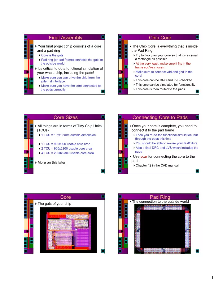
Final Assembly Chip Core Your final project chip consists of a core The Chip Core is everything that is inside and a pad ring the Pad Ring Core is the guts Try to floorplan your core so that it’s as small a rectangle as possible Pad ring (or pad frame) connects the guts to the outside world At the very least, make sure it fits in the frame you’ve chosen It’s critical to do a functional simulation of Make sure to connect vdd and gnd in the your whole chip, including the pads! core! Make sure you can drive the chip from the This core can be DRC and LVS checked external interface This core can be simulated for functionality Make sure you have the core connected to This core is then routed to the pads the pads correctly. Core Sizes Connecting Core to Pads All things are in terms of Tiny Chip Units Once your core is complete, you need to (TCUs) connect it to the pad frame 1 TCU = 1.5x1.5mm outside dimension Then you re-do the functional simulation, but through the pads this time You should be able to re-use your testfixture 1 TCU = 900x900 usable core area Also a final DRC and LVS which includes the 2 TCU = 900x2300 usable core area pads 4 TCU = 2300x2300 usable core area Use vcar for connecting the core to the pads! More on this later! Chapter 12 in the CAD manual Core Pad Ring The connection to the outside world The guts of your chip 1
The Connected Chip Tutorial Example A tiny state machine in a 1-tiny-chip frame Pad Cells Driving Large Capacitances Started with a set of pads from MOSIS Originally from Tanner Tools pads Problem: the pads don’t DRC, LVS, or simulate! Cameron Charles re-did the cells in 2002 (as a grad student) to fix these issues Result is UofU_Pads /uusoc/facility/cad_common/local/Cadence/lib/OA/UofU_Pads Use library manager to add this library Name it UofU_Pads They now DRC, LVS, and simulate! Using Cascaded Buffers How to Design Large Transistors ? 2
Tristate Buffers Bonding Pad Design Bonding Pad GND 100 µ m Out V DD Out In GND UofU_Pads UofU_Pads 255u Tanner Pads (prototype of UofU_Pads) UofU_Pads 3
UofU_Pads ESD and Analog Pads ESD Protection Pads from MOSIS ASIC Pads UofU_Pads pad_bidirhe Bidirectional pad with high enable pad_in Digital input pad pad_out Digital output pad pad_vdd, pad_gnd Power supply pads pad_io, pad_io_nores Analog pads (with and without series resistor) pad_nc, pad_space Non-connecting pad and spacer 4
Pad Interfaces pad_bidirhe pad_bidirhe pad_bidirhe (EN) (DataOut) (DataIn, DataInB) (pad) • DataOut drives a 78(p) x 45(n) inverter (30x) • Which then drives a 200(p) x 200(n) output driver (133x) Moderately complex pullup/pulldown • DataIn and DataInB come from 96(p) x 54(n) inverters (36x) structure • EN drives a 16(p) x 9(n) inverter (6x) • All signal pads are built from this one • All signals on are M2 pad_bidirhe pad_bidirhe Look at just the metal layers… EN, DataOut, DataInB, DataIn is the order Middle connection is direct connection to the pad (don’t use it!) M2 connections for EN, DataOut, DataIn, You put metal2 shape pins over the DataInB connection points (for icc) UofU Pads pad_out pad_out pad_out (pad) (DataOut) pad_in Like pad_bidirhe but with EN already tied pad_in (DataIn, DataInB) high for you (pad) All you need to connect is DataOut 5
pad_out pad_out You connect your signal to the DataOut You connect your signal to the DataOut connection into 78(p) x 45(n) inv (30x) connection into 78(p) x 45(n) inv (30x) pad_in pad_in Like pad_bidirhe but with EN tied low already for you Connect to the DataInB and DataIn port DataIn and DataInB provide input signals Driven from 94(p) x 54(n) inverters (36x) Power Supply Pads pad_vdd pad_vdd pad_vdd pad_gnd pad_gnd Vdd is on a big fat metal1 line 28.8u wide 6
pad_gnd More Pads GND is also on a big fat metal1 line Also 28.8u Timetable Available Frames Final Chip Assembly Frame1_38 Due Wednesday, December 14th Frame2h_70 Take the pad cells and make a pad ring Frame2v_70 Connect your working core to the pad ring Frame4_78, Frame4_80 Remember that Tiny Chip Units are 1,2,4 indicate how many Tiny Chip Units 1.5mm X 1.5mm and are not divisible h and v indicate horizontal and vertical for A 3.1mm X 2.8mm chip would cost 6 TCUs! the rectangular core frames Preference will go to the well-simulated _# indicates how many signal pins are chips available Secondary preference will be for the smaller Vdd and gnd are in the right spots – DON’T well-simulated chips MOVE THEM! Frame1_38 Frame1_38 40 pins total 40 pins total (38 signal pins) (38 signal pins) 10 on each side 10 on each side 990 x 990 core 990 x 990 core Save room for Save room for Routing to pads! Routing to pads! 900 x 900 900 x 900 Usable core Usable core 7
Frame1_38 Example Frame1 Chip 40 pins total (38 signal pins) 10 on each side 990 x 990 core Save room for Routing to pads! 900 x 900 Usable core Example Frame1 Chip Frame2h_68 72 pins total, 70 signal pins 990 x 2430 core (900 x 2300 usable) Frame2h_68 Frame4_78 72 pins total, 68 signal pins 990 x 2430 core (900 x 2300 usable) 84 total pins (78 signal pins) 2490 x 2490 (2300 x 2300 usable) 8
Frame4_78 How to Use the Rings Copy the pad ring of your choice /uusoc/facility/cad_common/local/Cadence/lib/OA/UofU_Pads From UofU_Pads To your project directory 84 total pins (78 signal pins) Leave the pad_vdd and pad_gnd where 2490 x 2490 (2300 x 2300 usable) they are! Select other pads, use properties to change to the pad type you want DON’T move them! Use pad_bidirhe, pad_out, and pad_in Frame Schematic Frame layout Frame1_38 with the right pads for the Frame1_38 with the right pads for the drink_machine drink_machine Pins Pins Frame1_38 with the right pads for the Frame1_38 with the right pads for the drink_machine drink_machine 9
Frame symbol Connect to Core Frame1_38 with the right pads for the Use this to start the ccar routing process drink_machine Layout with Virtuoso-XL Connect with icc Let ccar the routing Do placement, and connect vdd and gnd Vdd Connections Gnd Connections Notice how the pad frame is connected Notice how the pad frame is connected 10
Now Simulate the Whole Chip What Does This Mean? Use essentially the same testbench that For now, concentrate on getting your chip you used for the core core assembled, working, DRCed and This time you’ll be simulating with the pads in place LVSed. You’ll need to place one more set of pins so You need a working core before you need that the wholechip cell has connection points pads! Make sure your core fits in the pad ring that you want to use Then, use vcar to assemble the frame and core Simulate, LVS, DRC with the whole thing! Output to GDS (Stream) Fabrication Schedule MOSIS educational run Once everything is completely finished, Chips that go into the fab queue need to be you need to export the whole chip to GDS absolutely and completely ready to go: (stream) format Friday Jan 10 th at the LATEST Use the export->stream function in CIW There are a few more steps that projects use stream4gds.map as the Layer Map Table need to go through to make them fab-ready From even after DRC/LVS /uusoc/facility/cad_common/local/class/6710/F11/cadence/map_files If you make logos and names, those have to Fill in Library Name, Top Cell Name and Output File pass DRC too! Name Metal3 is recommended for logos… I will read this GDS file in and re-DRC that layout... Final Report Final Report Final Report, due Wed, December 14 Third: Standard Cells Standard Cell layouts, schematics, etc. Three parts: User’s guide First: Technical Paper (about project) Email .lib, .lef, and .v files to me at Not more than 10 pages teach-cs6710@list.eng.utah.edu IEEE two-column format Also tell me where your Cadence libraries are. Describe what makes your chip interesting I can slurp up the cell libraries if they are This is a self-contained paper of the form that readable by your group. might be submitted to a conference or journal Second: Project Details Floorplan, pinout, and system block diagram Schematics and layouts for all major parts A table of contents or readme guide 11
Recommend
More recommend
Explore More Topics
Stay informed with curated content and fresh updates.

