ASIC Physical Design Top-Level Chip Layout References: M. Smith, - PowerPoint PPT Presentation
ASIC Physical Design Top-Level Chip Layout References: M. Smith, Application Specific Integrated Circuits , Chap. 16 Cadence Virtuoso User Manual Top-level IC design process Typically done before individual circuit block layouts
ASIC Physical Design Top-Level Chip Layout References: M. Smith, Application Specific Integrated • Circuits , Chap. 16 Cadence Virtuoso User Manual •
Top-level IC design process Typically done before individual circuit block layouts Top-level netlists usually created before any layout Create top-level schematic “Components” are functional blocks and I/O pads Blocks include IP and user-created modules Create a chip “floor plan” from the schematic Place functional blocks and I/O pads Connections shown as overflows Route top-level connections (automatic or interactive) Eliminate overflows, DRC errors, shorts Create layouts of user-designed modules
Chip floorplan I/O pads
Modulo-7 counter in pad frame
Floorplanning (Smith text chap. 15, 16) Floorplanning: arrange major blocks prior to detailed layout to optimize chip area input is a netlist of circuit blocks (hierarchical) after system “partitioning” into multiple ICs estimate layout areas, shapes, etc. Flexible blocks – shape can be changed Fixed block – shape/size fixed do initial placement of blocks (keep highly-connected blocks close) decide location of I/O pads, power, clock
Floorplan a cell-based IC (Fig. 16.6) - may have to fit into “die cavity” in a package Heavy congestion below B Initial random floorplan Reduced congestion Blocks after moved to changes improve floorplan
Congestion analysis (Fig. 16.7) Initial 2:1.5 Altered to die aspect 1:1 aspect ratio ratio Trial floorplans A & B resized to reduce congestion Channel density Congestion map Change A & C to reduce congestion
Routing a T junction Constraining Preferred
Define channel routing order •Make “cuts” (slice in two) to separate blocks •Slicing tree, corresponding to sequence of cuts, determines routing order for channels - route in inverse order of cuts
Non-slicing structure Cyclic constraint Cannot find Slicing floorplan prevents channel slicing floorplan possible, but routing without increasing inefficient in use chip area of chip area
Power distribution Uses special power pads, wires, routing Option b: m1 parallel to Option a: longest side m1 for VSS --------------- m2 for VDD Easier routing --------- but more vias Potential problems in routing channel Array of via Many layer contacts for changes/vias VDD/VSS if VDD/VSS Buses. on different layers
Clock distribution (minimize skew) Often use “clock tree” structure
MOSIS SCMOS Pad Library Includes 6 pad types: Input & output pads with buffers VDD & GND pads with ESD Analog IO pad with ESD Analog reference pad with ESD Assemble into a “frame” in which pads butt against each other Allows VDD & GND wires to form a continuous ring Special “spacer” and “corner” pads complete the ring ADK tools will generate a pad frame from a schematic
MOSIS 15 14 13 12 11 10 9 8 7 6 Tiny Chip TSMC 0.35um Pin #’s Hi-ESD Pad Frame 5 16 4 17 3 18 (l) lambda=0.30um 2 19 1 20 40 21 39 22 38 23 37 24 36 25 26 27 28 29 30 31 32 33 34 35
MOSIS TSMC 0.35um Hi-ESD Pad Frame VDD/GND Physical layout wires form continuous ring through the pad frame Spacer pad if no signal Corner pad (passes VDD/GND)
MOSIS I/O Pad Schematic Inputs to logic ckts Output enable Bonding Pad Outputs from logic ckts
Simplified pad circuit
MOSIS 1.6 um bidirectional pad Source: Weste, “CMOS VLSI Design” To Core
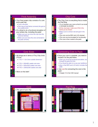
ASIC frame + core in Virtuoso Process: 1. Create “core” block 2. Create pad frame 3. Connect them
Top-level bottom-up design process Generate block layouts and for each block: Import the GDSII (or DEF) stream into a Virtuoso library Import the Verilog netlist into the library Perform DRC and LVS on each block until “clean” Create a schematic symbol from the netlist in the library Create a block diagram/schematic in Virtuoso “Composer” Create a library for the top-level circuit block and create a schematic view Instantiate schematic symbols from the library Interconnect with nets and add pins Check and save Create a layout from the schematic diagram
Top-level block schematic in “Composer”
Before module and I/O placement Blocks initially outside boundary
After placing modules and pins
Power routing between blocks Connect power rings
Nets shown as “overflows”
Routed circuit block
Block symbol (to connect to I/O pads)
Pad frame with signal wires
Zoomed view of pad frame
Schematic: block + pad frame
Placement of frame and core
Power/ground routed manually
Before signal routing
After routing – final layout
Recommend
More recommend
Explore More Topics
Stay informed with curated content and fresh updates.

