ASIC Chip Layout with UofU Cadence Design Kit References: Erik - PowerPoint PPT Presentation
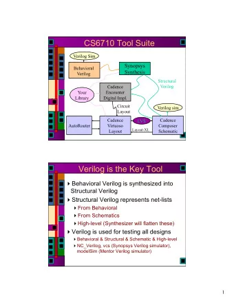
ASIC Chip Layout with UofU Cadence Design Kit References: Erik Brunvand, Digital VHDL Chip Design with Cadence and Synopsys CAD Tools Cadence Virtuoso User Manual Setup for NCSU/UofU ami06 .bashrc environment variables # Set up
ASIC Chip Layout with UofU Cadence Design Kit References: Erik Brunvand, Digital VHDL Chip Design • with Cadence and Synopsys CAD Tools Cadence Virtuoso User Manual •
Setup for NCSU/UofU ami06 .bashrc environment variables # Set up NCSU-CDK and Univ. of Utah Support export CDK_DIR=/class/ELEC6250/ncsu-cdk-1.6.0.beta export SYSTEM_CDS_LIB_DIR=/home/nelson/nelsovp Your home directory export CDS_NETLISTING_MODE=Analog # Create alias for Global Foundries BICMOS8HP Digital Kit export CMOS8HP=/class/ELEC6250/cmos8hp/std_cell/v.20130404 BICMOS8HP export BICMOS8HP=/class/ELEC6250/IBM_PDK/bicmos8hp/relHP setup export TECHDIR=/class/ELEC6250/IBM_PDK/bicmos8hp/relHP/Calibre From directory /class/ELEC6250/UofUtah Copy cdsinit to your home directory and name it .cdsinit (this will load other initialization files) Copy cds.lib.auburn to your home directory or to your project directory (or add lines from this file to your current cds.lib file) Example on next slide.
cds.lib Virtuoso loads cds.lib from the directory in which it is invoked cds.lib in my home directory has the “system library” definitions for the installed libraries (BICMOS8HP , NCSU, UofU, Cadence, etc.) cds.lib in my project directory references the above and then defines my own project-specific libraries: SOFTINCLUDE /home/nelson/nelsovp/cds.lib DEFINE UofU_tricounter /home/nelson/nelsovp/cadence/Modulo6_UofU/top/UofU_tricounter DEFINE my_new_ami06 /home/nelson/nelsovp/cadence/Modulo6_UofU/top/my_new_ami06 DEFINE my_pads /home/nelson/nelsovp/cadence/Modulo6_UofU/top/UofU_Pads Pads copied from UofU installation
NCSU Cadence Design Kit (CDK) https://www.eda.ncsu.edu/wiki/NCSU_CDK For analog/digital CMOS IC design via the MOSIS IC fabrication service (www.mosis.org) Version ncsu-cdk-1.6.0.beta for Cadence Virtuoso 6.1 and later Supports all MOSIS processes based on SCMOS rules ami_06/16, hp_04/06, tsmc_02/03/04 GDSII layer maps Diva DRC, LVS support (no PEX) Composer interfaces to HSPICE/Spectre, Verilog Technology-independent libraries for analog & digital parts Transistor models, layouts, etc. But – does not include standard cell layout library MOSIS wirebond pads (AMI 0.6 μ m, TSMC 0.4 μ m, HP 0.6 μ m) Installed in /class/ELEC6250/ncsu-cdk-1.6.0.beta
U. of Utah CDK (used in Dr. Brunvand’s book) /class/ELEC6250/UofUtah/ UofU_TechLib_ami06 UofU-modified tech library for AMI C5N 0.5 micron CMOS process, in the NCSU CDK framework (AMI acquired by ON Semiconductor for $915M in 2008) UofU_Digital_v1_2 Std. Cell library (37 cells, use M1 & M2) UofU_Digital_v1_2.db: compiled library file for Synopsys Design Compiler UofU_Digital_v1_2.lef: abstract layout information file for place and route tools UofU_Digital_v1_2.lib: library characterization file UofU_Digital_v1_2.v:Verilog interface and simulation behavior file UofU_Digital_v1_2_behv.v:Verilog models with timing “specify” blocks UofU_Pads Pad cells and frames based on the MOSIS-supplied .5 μ m pads from Tanner, but UofU-modified to pass DRC and LVS UofU_AnalogParts UofU-modified transistor models that add delay to the switch-level simulation of those devices
UofU_Digital_v1_2 CMOS cell library AND3X1: 3-input AND AOI21X1, AOI22X1:AND-OR-Invert gates Xn = drive strength BUFX2, BUFX4, BUFX8: non-inverting buffers DCBNX1, DCBX1, DCNX1, DCX1: D-type flip flops with active-low clear. B means that the device includes both Q and QB outputs. N means active-low clock. ENINVX1, ENINVX2: enabled (tri-state) inverters FILL, FILL2, FILL4, FILL8: filler cells of different widths for filling in std cell rows INVX1, INVX16, INVX2, INVX4, INVX8: inverters LCNX1, LCX1: level-sensitive (gated) latches with active-low clear. N means active-low gate MUX2NX1, MUX2X2: 2-way muxes. N means an inverting mux NAND2X1, NAND2X2, NAND3X1: NAND gates with 2 and 3 inputs NOR2X1, NOR2X2, NOR3X1: NOR gates with 2 and 3 inputs OAI21X1 OAI22X1: OR-AND-Invert gates TIEHI, TIELO: Cells used to tie inputs high or low XNOR2X1: 2-input XNOR XOR2X1: 2-input XOR
UofU_Digital_v1_2 cell views Cells use UofU_TechLib_ami06 technology library cmos_sch – schematic of transistors from UofU_Analog_Parts library behavioral -Verilog with “specify” blocks for SDF simulation layout – full cell layout symbol – to use in gate-level schematics extracted – extracted from layout for LVS verification
UofU_Pads Based on MOSIS-supplied .5 μ m pads from Tanner • Frame1_38 for MOSIS “TinyChip” (38 signal pins, 2 power/ground pins) • Layout and schematic views • Edit properties to change pad type within the frame • Power/ground: pad_vdd, pad_gnd • Signal: pad_in, pad_out, pad_io • No connect: pad_nc • Corner: pad_corner
UofU_Analog_Parts Based on NCSU_Analog_Parts nmos/pmos 3-terminal (bulk to gnd!/vdd!) bi_nmos/bi_pmos bidirectional device r_nmos/r_pmos weak/resistive transistors vdd/gnd
BICMOS8HP/UofU differences Synthesis with Synopsys Design Compiler Setup file: .synopsys_dc.setup Path to library: /class/ELEC6250/UofUtah Target library: UofU_Digital_v1_2.db Synthesis script references to specific library cells Example: myInputBuf (cell driving inputs) Example: Synthesized Modulo-6 counter netlist
BICMOS8HP/UofU differences Block layout with Innovus Technology: 500 nm feature size (BICMOS8HP is 130 nm) Wires/spacing may have to be larger Special library cells (filler, clock buffer, etc.) LEF file: UofU_Digital_v1_2.lef Power: vdd! Ground: gnd! Timing library: UofU_Digital_v1_2.lib (no capacitance table) I/O pins and routing with only 3 metal layers: M1 M2 M3 Power planning nets: vdd! gnd! See later slide for exporting layout to Virtuoso Example: Modulo-6 counter layout (next slide)
Innovus: modulo6 in ami06 technology 3 metal layers
Innovus: save cell for importing into Virtuoso Export DEF (Design Exchange Format) file: Menu: File > Save > DEF Command: global dbgLefDefOutVersion set dbgLefDefOutVersion 5.6 defOut -floorplan -netlist -routing $BASENAME.def Export Verilog structural netlist Menu: File > Save > Netlist Command: saveNetlist -phys -includePowerGround -excludeLeafCell ${BASENAME}_soc.v
Virtuoso CIW (Command Interpreter Window) Cadence libraries and tools are accessed from the CIW Import/Export designs Access libraries
Library Manager New cell Library paths in cds.lib Views created by import. Double click to open with appropriate tool. New library
Import digital block into Virtuoso Create a new Cadence library for the cell Attach technology library UofU_TechLib_ami06 Import DEF layout information into Virtuoso: Innovus saved: mydesign.def Import into a the new Cadence library File > Import > DEF Results in cell “layout” view Import circuit netlist into Virtuoso: Gate-level netlist saved by Innovus: mydesign.v Import netlist into a Cadence Library File > Import > Verilog Results in cell “schematic” and “symbol” views
In Virtuoso CIW: File > New > Library My library name Directory for library files Attach to an existing library Select UofU_TechLib_ami06
In Virtuoso CIW: File > Import > DEF my_new_ami06 DEF file from Innovus My library for this cell Name of top design cell Cell view type Technology library (Contains std. cells & .lib/.lef/.v files)
In Virtuoso CIW: File > Import > Verilog My library for this cell Reference tech libraries Verilog file(s) Verilog models of UofU_Digital_v1_2_behv.v the standard cells (copy to your directory) Create schematic and symbol views
Schematic view of “modulo6”
Symbol view of “modulo6”
Layout view of “modulo6” Abstract view- no cell layout details
Verify the layout (DRC-Extract-LVS) First - change cellviews of instances from abstract to layout Tools > Find/Replace Click to add view name Instances (inst) Change view name from abstract to layout Replace all
Layout view of “modulo6” Layout details now shown To see all layers: Options>Display Display levels Start 0 Stop 30
Design rule check to ensure correct layout Verify > DRC Design rules file No violations!
Extract to prepare for LVS Verify > Extract Extraction rules file “extracted” view added to cell
Perform layout vs schematic check Verify > LVS Browse to select schematic & extracted cell views from library LVS rules file
Top-level bottom-up design process Generate block layouts and for each block: Create a Virtuoso library for each block Import DEF file and Verilog netlist Perform DRC-Extract-LVS on each block until “clean” Create a block diagram schematic in Virtuoso Schematic Create a library for the top-level block Create a schematic view Instantiate schematic symbols from the library Interconnect with nets and add pins Check and save Create a layout from the schematic diagram
Top-level block schematic in “Schematics XL” Layout blocks
Recommend
More recommend
Explore More Topics
Stay informed with curated content and fresh updates.







![N -Alkyl- N -[5-(propylamino)-9 H -benzo[ a ]phenoxazin-9-ylidene]alkan-1- aminium chlorides:](https://c.sambuz.com/711267/n-alkyl-n-5-propylamino-9-h-benzo-a-phenoxazin-9-ylidene-s.webp)


