An Interconnect-Centric Design Flow for Nanometer Technologies - PDF document
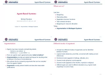
An Interconnect-Centric Design Flow for Nanometer Technologies Jason Cong UCLA Computer Science Department Email: cong@cs.ucla.edu Tel: 310-206-2775 http://cadlab.cs.ucla.edu/~cong Outline Global interconnects in nanometer technologies
An Interconnect-Centric Design Flow for Nanometer Technologies Jason Cong UCLA Computer Science Department Email: cong@cs.ucla.edu Tel: 310-206-2775 http://cadlab.cs.ucla.edu/~cong Outline � Global interconnects in nanometer technologies � Interconnect-centric design flow � Physical hierarchy generation � Motivation � Approaches � Results and on-going work Jason Cong 10/17/01 2
Interconnect Delays in Nanometer Technologies Technology (um) 0.25 0.18 0.15 0.13 0.10 0.07 Intrinsic gate delay (ps) 71 51 49 45 39 22 1mm (ps) 59 49 51 44 52 42 2cm no-opt (ps) 2600 2500 2700 2600 3700 4700 900 800 770 700 770 670 2cm best-opt (ps) • Best-opt uses simultaneous buffer insertion, driver/buffer sizing, and wiresizing • Based on NTRS’97 data, with consideration of use copper & low-K materials Fact: Global interconnect is 15x – 20x slower than logic gates Jason Cong 10/17/01 3 How Far Can We Go in Each Clock Cycle 7 clock � NTRS’97 0.07um Tech � 5 G Hz across-chip clock 6 clock � 620 mm 2 (24.9mm x 24.9mm) � IPEM BIWS estimations � Buffer size: 100x 5 clock � Driver/receiver size: 100x � From corner to corner: � 7 clock cycles 4 clock 3 clock 1 clock 2 clock Jason Cong 15.04 22.56 24.9 (mm) 10/17/01 4 0 7.52
Two Important Implications � Interconnects determine the system performance Interconnect/communication-centric design methodology � Need multiple clock cycles to cross the global interconnects in giga-hertz designs Pipelining/retiming on global interconnects Jason Cong 10/17/01 5 Interconnect-Centric Design Methodology � Proposed transition interconnect device device interconnect device/function centric interconnect/communication centric � Analogy Data/Objects Programs Programs Data/Objects Jason Cong 10/17/01 6
Interconnect-Centric IC Design Flow Under Development at UCLA Architecture/Conceptual-level Design Design Specification Interconnect Planning Interconnect Performance • Physical Hierarchy Generation Estimation Models (IPEM) HDM • Foorplan/Coarse Placement with Interconnect Planning • OWS, SDWS, BISWS • Interconnect Architecture Planning abstraction Synthesis and Placement under Physical Hierarchy Structure view Functional view Interconnect Optimization Interconnect Synthesis Physical view (TRIO) Topology genration & wiresizng for delay Timing view • Topology Optimization with Buffer Insertion • Wire sizing and spacing • Simultaneous Buffer Insertion and Wire Sizing Wire ordering & spacing for noise control • Simultaneous Topology Construction with Buffer Insertion and Wire Sizing Interconnect Layout Route Planning Point-to-Point Gridless Routing Jason Cong 10/17/01 7 Final Layout Interconnect Planning • Current approach: • RT-level floorplanning based on logic hierarchy Delay budgeting + block by block synthesis + physical design • Jason Cong 10/17/01 8
Example of Logic Hierarchy Verilog module cpu(pj_su, pj_boot8, …); SRAM input …; dtag output …; ICRAM DCRAM fpu fpu(.fpain (iu_rs2_e), .fpbin(iu_rs1_e), .fpop(fpop), SMU DCU .fpbusyn(fp_rdy _e), .fpkill(iu_kill_fpu), PCSU .fpout(fpu_data_e), .clk (clk), …); pcsu pcsu(.pj_clk_out(pj_clk _out), …); ICU smu smu(.i u_optop_in(iu_optop_din), …); Integer Unit dtag_shell dtag_shell(.tag_in(dcu_tag_in), …); (IU) dcram_shell dcram_shell(.data_in({dcu_din_e[31], …); itag dcu dcu( .biu_data(pj_datain ), …); itag_shell itag_shell(.icu_tag_in(icu_tag_in), …); icram_shell icram_shell(.icu_din(icu_din), …); FPU MEMORY icu icu(.biu_data(pj_datain), …); iu iu(.iu_data_vld(iu_data_vld ), …); endmodule latches Jason Cong 10/17/01 9 Interconnect Planning • Current approach: • RT-level floorplanning based on logic hierarchy Delay budgeting + block by block synthesis + physical design • • Problem: may loss much optimality • Logic hierarchy may not embed well on a 2D silicon surface, resulting poor global interconnect Jason Cong 10/17/01 10
Example of Logic Hierarchy in Final Layout By courtesy of IBM (Tony Drumm) Jason Cong 10/17/01 11 Example of Logic Hierarchy in Final Layout By courtesy of IBM (Tony Drumm) Jason Cong 10/17/01 12
Interconnect Planning Current approach: • RT-level floorplanning based on logic hierarchy • • Delay budgeting + block by block synthesis + physical design • Problem: may loss much optimality • Logic hierarchy may not embed well on a 2D silicon surface, resulting poor global interconnect • Our conclusion: • RT-level floorplanning of logic blocks may be a bad idea • Our proposal: • synthesis under physical hierarchy Jason Cong 10/17/01 13 Physical Hierarchy Generation Problem Formulation Logical Hierarchy Hard IP Soft module Assign modules to physical hierarchy with interconnect estimation and optimization Same color for modules of the same logic hierarchy Jason Cong 10/17/01 14
Impact of Physical Hierarchy Generation Define the Global Interconnects Latch Critical path Example: Global interconnects defined by two different physical hierarchies Jason Cong 10/17/01 15 Synthesis under Physical Hierarchy A=3 D=4 A=4 D=3 Alternative Architecture Block Selection Latch Re-Synthesis and Retiming Critical path Jason Cong 10/17/01 16
Difficulties in Physical Hierarchy Generation � How to consider retiming/pipelining over global interconnects Use of the concepts of sequential arrival/required times � How to handle the high complexity of “almost flattened” designs Use the multi-level optimization technique Jason Cong 10/17/01 17 Need of Considering Retiming during Placement - Retiming/pipelining on global interconnects � Multiple clock cycles are needed to cross the chip � Proper placement allows retiming to hide global interconnect delays . Placement 1 Placement 2 d b c a c d a b d(v)=1, WL=6, d(e) ? WL d(v)=1, WL=6, d(e) ? WL Before retiming, ? = 4.0 Before retiming, ? = 5.0 Better Initial Placement !! After retiming, ? = 3.0 Jason Cong 10/17/01 18
Need of Considering Retiming during Placement - Retiming/pipelining on global interconnects � Multiple clock cycles are needed to cross the chip � Proper placement allows retiming to hide global interconnect delays . Placement 1 Placement 2 d b c c d a a b d(v)=1, WL=6, d(e) ? WL d(v)=1, WL=6, d(e) ? WL Before retiming, ? = 4.0 Before retiming, ? = 5.0 Better Initial Placement !! After retiming, ? = 3.0 After retiming, ? = 4.0 Jason Cong 10/17/01 19 Sequential Arrival Time (SAT) � Definition [Pan et al, TCAD98] � l ( v ) = max delay from PIs to v after opt. retiming under a given clock period f � l ( v ) = max{ l ( u ) - f · w ( u,v ) + d ( u,v ) + d ( v )} u v l ( u ) w ( u,v ) d ( v ) � Relation to retiming: r ( v ) = ? l ( v ) / f ? - 1 � Theorem: P can be retimed to f + max{ d ( e )} iff l (POs) ? f l ( u ) = 7 u d ( v ) = 1, d ( e ) = 2, f = 5 v l ( v ) = max{7-5·1+2+1, 3+2+1} = 6 l ( w ) = 3 w Jason Cong 10/17/01 20
Sequential Arrival Time (SAT) Computation � Difficulty � Need to work on the entire circuit, with many cycles � Topological order does not exist! � Basic approach: � Start with min l -value for each node and iteratively improve it � Will the computation converge? � YES, if the the circuit can be retimed to the target cycle time � Theorem: Convergence is guaranteed in O(n) iterations if the circuit can be retimed to the target cycle time � Practical experience � Converge in constant iterations with a good DFS order Jason Cong 10/17/01 21 Example: SAT Computation a d(v)=1, d(e)=2 d Is ? = 4.5 possible ? c e g b f Iter# a b c d e f g - ? - ? - ? - ? - ? 0 0 0 - ? - ? - ? - ? 1 0 0 -1.5 - ? - ? 2 0 0 -1.5 1.5 1.5 3 0 0 -1.5 1.5 4.5 0 0 4 0 0 -1.5 1.5 4.5 0 0 5 0 0 -1.5 1.5 4.5 0 0 l (g) ? 4.5 Cycle time 4.5 is possible as Jason Cong 10/17/01 22
Example: SAT Computation a d(v)=1, d(e)=2 d Is ? = 4.5 possible ? c e g b f Iter# a b c d e f g - ? - ? - ? - ? - ? 0 0 0 - ? - ? - ? - ? 1 0 0 -1.5 - ? - ? 2 0 0 -1.5 1.5 1.5 3 0 0 -1.5 1.5 4.5 0 0 4 0 0 -1.5 1.5 4.5 0 0 5 0 0 -1.5 1.5 4.5 0 0 l (g) ? 4.5 Cycle time 4.5 is possible as Jason Cong 10/17/01 23 Simultaneous (Coarse) Placement with Retiming on Interconnects � Our solution � Compute SATs of all nodes for a given placement solution � Minimize SATs of POs by improving the placement solution � Alternative solution [Brayton, et al] � Enforcing all loop constraints during placement Jason Cong 10/17/01 24
Difficulties in Physical Hierarchy Generation � How to consider retiming/pipelining over global interconnects Use of the concepts of sequential arrival/required times � How to handle the high complexity of “almost flattened” designs Use the multi-level optimization technique Jason Cong 10/17/01 25 Multi-Level Framework Levels Uncoarsening & Coarsening Refinement (optimization) Problem sizes • Multi-level coarsening generates smaller problem sizes for top levels � faster optimization on top levels • Different levels explore different aspects of the solution space • Refinement on good solutions from coarser levels can be fast and simple with good solution quality Jason Cong 10/17/01 26
Recommend
More recommend
Explore More Topics
Stay informed with curated content and fresh updates.
