Pushing Ultra-Low-Power Digital Circuits into the Era Nanometer - PowerPoint PPT Presentation
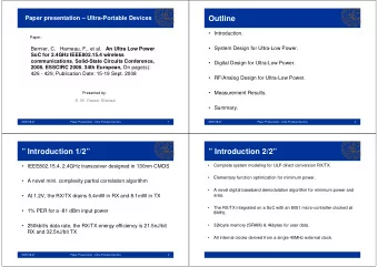
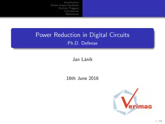
Pushing Ultra-Low-Power Digital Circuits into the Era Nanometer David Bol Microelectronics Laboratory Ph.D public defense December 16, 2008 Pushing Ultra-Low-Power Digital Circuits into the Era Nanometer David Bol Microelectronics
Pushing Ultra-Low-Power Digital Circuits into the Era Nanometer David Bol Microelectronics Laboratory Ph.D public defense December 16, 2008
Pushing Ultra-Low-Power Digital Circuits into the Era Nanometer David Bol Microelectronics Laboratory Ph.D public defense December 16, 2008
Why ultra-low power ? Low-power circuits Performances: 1 GOp/s Power < 1 W High-performance circuits Performances: 10 GOp/s Power < 100 W 2 D. Bol
Hearing aids D. Bol
ULP digital circuits Hearing aids and biomedical RFID tags Ultra-low-power circuits Performances: 10 k - 10 MOp/s Sensor Power < 1µW Wearable networks electroncics Smart Dust [Berkeley] 3 D. Bol
Pushing Ultra-Low-Power Digital Circuits into the Era David Bol Microelectronics Laboratory Ph.D public defense December 16, 2008
Moore’s law (1965) Every 18 months : x 2 [Intel] 5 D. Bol
Moore’s law today 6 D. Bol
Moore’s law Moore’s law without technology scaling Moore’s law with technology scaling 7 D. Bol
Technology scaling Clock frequency 2008 130n 1 GHz 45nm 100 MHz 10 MHz 1 MHz 10 4 10 5 10 6 10 7 10 8 10 9 Transistor count 8 D. Bol
Technology scaling Clock frequency 2008 130n 1 GHz 45nm 100 MHz ULP circuits 10 MHz ? 1 MHz 10 4 10 5 10 6 10 7 10 8 10 9 Transistor count 8 D. Bol
Trend in ULP digital circuits Last chips [IEEE ISSCC’08]: 400 m n 5 6 300 Technology node [nm] Ultra-low-power 0.3V µC for 200 biomedical applications [Kwong] ITRS 100 65nm Ultra-low-power 0.32V 0 1998 2000 2002 2004 2006 2008 motion estimator [Kaul] Year 9 D. Bol
Outline • Motivation • Basics: energy consumption of ULP digital circuits • Impact of technology scaling • Reaching E min • Reducing E min • ULP logic style for high-temperature applications • Roadmap for nanometer ULP circuits D. Bol
Sources of power dissipation V dd I on 1/f clk OUT IN ‘1’ ‘0’ C L 10 D. Bol
Sources of power dissipation V dd 1/f clk OUT IN ‘0’ ‘1’ I on C L 10 D. Bol
Sources of power dissipation V dd 1/f clk OUT IN ‘0’ ‘1’ I on C L P dyn ~ f clk x C L x V dd2 10 D. Bol
Sources of power dissipation V dd IN OUT ‘0’ ‘1’ I on C L P dyn ~ f clk x C L x V dd2 kg 11 D. Bol
Power consumption 8-bit RCA multiplier in 130nm technology 1.5 ULP applications Minimum V dd [V] Speed = subthreshold logic limit 1 Functional limit 0.5 0 4 5 6 7 8 9 10 10 10 10 10 10 -3 10 2 P dyn ~ f clk x C L x V dd Power [W] -5 g 10 Frequency scaling n i l a c s e g a t l o -7 v / 10 y c n e u q e r F -9 10 4 5 6 7 8 9 10 10 10 10 10 10 Throughput [Op/s] 12 D. Bol
Sources of power dissipation V dd I off = I leak IN OUT ‘0’ ‘1’ C L P stat ~ V dd x I leak 13 D. Bol
Power consumption 8-bit RCA multiplier in 130nm technology 1.5 ULP applications Minimum V dd [V] Speed = subthreshold logic limit 1 Functional limit 0.5 0 4 5 6 7 8 9 10 10 10 10 10 10 -3 10 2 P dyn ~ f clk x C L x V dd e g a Power [W] -5 t l o 10 v / ULP applications y c n e g u n q i l a e c r F s -7 10 P stat = V dd x I leak -9 10 4 5 6 7 8 9 10 10 10 10 10 10 Throughput [Op/s] 14 D. Bol
Energy consumption 8-bit RCA multiplier in 130nm technology 1.5 ULP applications Minimum V dd [V] Speed = subthreshold logic limit 1 Functional limit 0.5 0 4 5 6 7 8 9 10 10 10 10 10 10 Energy per operation [J] -12 2 E dyn ~ C L V dd 10 ULP applications e g a t E min l o v / y -13 c n 10 e g u n q i l a e E stat c r F s -14 10 4 5 6 7 8 9 10 10 10 10 10 10 Throughput [Op/s] 15 D. Bol
Outline • Motivation • Basics: energy consumption of ULP digital circuits • Impact of technology scaling • Reaching E min • Reducing E min • ULP logic style for high-temperature applications • Roadmap for nanometer ULP circuits D. Bol
Impact of technology scaling Gate Gate Source Drain T ox W Source Drain L L T ox , L , W ~ 1/S Gate W T ox L Source Drain L 16 D. Bol
Impact of technology scaling Reduce V dd • I on Speed • C L kg • I leak 2 E dyn ~ C L V dd 2 E stat ~ I leak V dd • Variability ! Gate W T ox L Source Drain L 17 D. Bol
r i a b i l i t y � a r r r 130nm technology Gate Gate Gate Source Drain Source Drain Continuous doping Straight line edges 45nm technology Gate Rough line edges Source Drain Discrete dopants 17 D. Bol
Impact of technology scaling 8-bit RCA multiplier 1.5 Minimum V dd [V] Speed limit 1 Functional m n 0 3 0.5 limit 1 m n 5 4 0 4 5 6 7 8 9 10 10 10 10 10 10 -10 Energy per operation [J] 10 Variability -11 10 45nm E dyn -12 10 -13 10 1 3 0 n m -14 10 4 5 6 7 8 9 10 10 10 10 10 10 Throughput [Op/s] 18 D. Bol
Impact of technology scaling 8-bit RCA multiplier 1.5 Minimum V dd [V] Speed limit 1 Functional m n 0 3 0.5 limit 1 m n 5 4 0 4 5 6 7 8 9 10 10 10 10 10 10 -10 Energy per operation [J] 10 ULP applications -11 10 45nm E dyn -12 10 E stat -13 10 1 3 0 n m -14 10 4 5 6 7 8 9 10 10 10 10 10 10 Throughput [Op/s] 18 D. Bol
Impact of technology scaling Energy per operation x10 ! Energy per operation ULP applications 45nm m n 0 3 1 E min 2 1 Throughput 19 D. Bol
What if you have to scale ? What if you have to scale ? Scale, scale, scale… Famous Intel co-founder Y I D D. Bol
Outline • Motivation • Basics: energy consumption of ULP digital circuits • Impact of technology scaling • Reaching E min 1 • Reducing E min 2 • ULP logic style for high-temperature applications • Roadmap for nanometer ULP circuits D. Bol
Technology versatility 1 High-Performance/ General-Purpose • Short L g • High I on • Thin T ox • High I leak • Low V t • Mid V dd 45nm technology Low-Power • Mid L g • Low I on • Mid T ox • Low I leak • High V t • High V dd 21 D. Bol
Technology selection 1 8-bit RCA multiplier in 45 nm technology 0.8 Minimum V dd [V] LP 0.6 high-V t high-V t 0.4 GP General- 0.2 Purpose 0 4 5 6 7 8 10 10 10 10 10 -12 10 Energy per operation [J] GP LP -13 10 Low- Power ULP applications -14 10 4 5 6 7 8 10 10 10 10 10 Throughput [Op/s] 22 D. Bol
Dual-V t assignement Std-V t Non-critical path Register Register Non-critical path clk clk 23 D. Bol
Dual-V t assignement Std-V t Non-critical path Register Register High-V t Non-critical path High-V t clk clk 23 D. Bol
Dual-V t assignement A B High-V t Critical path OUT IN Mult Std-V t N OUT 40 Typical 32 With variability 27 30 Maximum N 19 20 11 Inefficient 8 7 10 3 2 0 0.2 0.4 0.6 0.8 1 1.2 V dd [V] 24 D. Bol
Circuit adaptation 1 +40% • Global process variations • Temperature variations +90% Energy per operation • Modeling errors a c t • Device aging u a l model target throughput 25 D. Bol
Circuit adaptation 1 Energy per operation a c t u a l model adapt. target throughput 25 D. Bol
Circuit adaptation 1 8-bit benchmark multiplier in 45 nm LP technology 0.5 0.6 a c t u a l 0.3 0.4 adapt V BB [V] V dd [V] 0 0.3 -0.3 target throughput 0.2 -0.6 0.1 1 10 2 V dd ASV (V BB =0V) Norm. energy per op. +70% 1.8 ABB (V dd =0.35V) V dd -V BB 1.6 1.4 1.2 V BB 1 0.8 0.1 1 10 Norm. throughput 26 D. Bol
Circuit adaptation 1 8-bit benchmark multiplier in 45 nm LP technology 0.5 0.6 a c t u Minimum V BB [V] a l 0.3 dd [V] adapt 0.4 Minimum V 0 0.3 ASV (V BB =0V) -0.3 target throughput ABB (V dd =0.35V) 0.2 -0.6 0.1 1 10 2 V dd Norm. energy per op. 1.8 V dd -V BB 1.6 ABB better 1.4 1.2 V BB ASV 1 better 0.8 0.1 1 10 Norm. throughput 26 D. Bol
Circuit adaptation 1 8-bit benchmark multiplier in 45 nm LP technology 0.5 0.6 a c t u Minimum V BB [V] a l 0.3 dd [V] adapt 0.4 Minimum V 0 0.3 ASV (V BB =0V) -0.3 target throughput ABB (V dd =0.35V) 0.2 -0.6 0.1 1 10 Reverse body bias 2 Norm. energy per op. is fine in 45 nm LP 1.8 technology 1.6 ABB better 1.4 Problem in 45 nm GP! 1.2 ASV What at 32 nm? 1 better 0.8 0.1 1 10 Norm. throughput 26 D. Bol
Outline • Motivation • Basics: energy consumption of ULP digital circuits • Impact of technology scaling • Reaching E min 1 • Reducing E min 2 • ULP logic style for high-temperature applications • Roadmap for nanometer ULP circuits D. Bol
E min modeling 90nm 45nm [Hanson, IEEE TED, pp. 175-185, 2008] D. Bol
Evolution of E min New effects in nanometer technologies 60 C L S 2 50 40 E min [fJ] In all 30 flavors 20 10 0 130nm 90nm 65nm 45nm 28 D. Bol
New effects in nanometer technologies 60 50 C L S 2 40 E min [fJ] 30 Var. 30 20 I gate 10 DIBL 25 New effects: 0 130nm 90nm 65nm 45nm S short • Bad short-channel S S long 20 E min [fJ] • Drain-induced barrier lowering 15 • Gate leakage 10 • Variability C L S 2 5 Gate I gate 0 Bulk Bulk opt. Source Drain DIBL 29 D. Bol
Recommend
More recommend
Explore More Topics
Stay informed with curated content and fresh updates.
