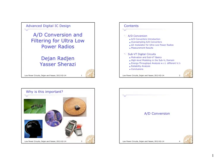
A/D Conversion and A/D Conversion Filtering for Ultra Low - PowerPoint PPT Presentation
Advanced Digital IC Design Contents A/D Conversion and A/D Conversion Filtering for Ultra Low Filtering for Ultra Low A/D Converters Introduction Oversampling A/D Converters Power Radios modulator for Ultra Low Power Radios Measurement
Advanced Digital IC Design Contents A/D Conversion and A/D Conversion Filtering for Ultra Low Filtering for Ultra Low A/D Converters Introduction Oversampling A/D Converters Power Radios ΔΣ modulator for Ultra Low Power Radios Measurement Results Sub-VT Digital Circuits Dejan Radjen Dejan Radjen Motivation and Sub-VT Basics High-level Modeling in the Sub-V T Domain Yasser Sherazi Energy-Throughput Analysis w.r.t. different V T ’s Reliability Analysis Conclusions Low Power Circuits, Dejan and Yasser, 2012-02-14 1 Low Power Circuits, Dejan and Yasser, 2012-02-14 2 Why is this important? A/D Conversion Low Power Circuits, Dejan and Yasser, 2012-02-14 3 Low Power Circuits, Dejan and Yasser, 2012-02-14 4 1
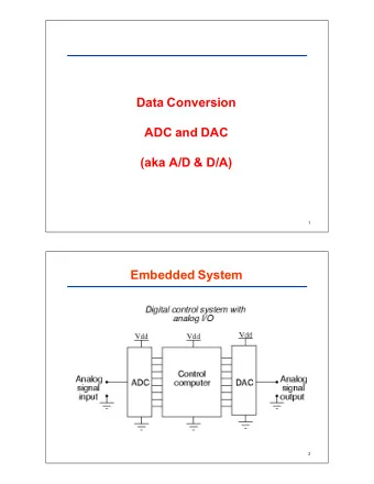
A/D converters introduction A/D converters introduction White noise approximation accuracy Accurate for rapidly changing and random input signals Increases with the number of bits in the quantizer Increases with the number of bits in the quantizer Least accurate for 1-bit quantizers but used anyway Maximum theoretical SNR for an N-bit ideal ADC = + SQNR 6.02 N 1.76 dB Low Power Circuits, Dejan and Yasser, 2012-02-14 5 Low Power Circuits, Dejan and Yasser, 2012-02-14 6 Oversampling A/D Converters Oversampling A/D Converters Basic principle of oversampling Basic principle of oversampling Low Power Circuits, Dejan and Yasser, 2012-02-14 7 Low Power Circuits, Dejan and Yasser, 2012-02-14 8 2
Oversampling A/D Converters Oversampling A/D Converters ΔΣ modulation for A/D conversion SQNR controlled by Order of the loop filter Number of bits in the quantizer Number of bits in the quantizer Oversampling ratio ΔΣ ADCs vs. Nyquist ADCs + High resolution obtained with few bits in the quantizer + Mismatch in the quantizer suppressed by the loop General ΔΣ -modulator Linear model - Additional analog blocks in the loop filter - Feedback loop → stability issues Feedback loop stability issues = + ( ) ( ) ( ) ( ) ( ) Y z STF z X z NTF z E z Signal Transfer Function: STF z ( ) Noise Transfer Function: NTF z ( ) Low Power Circuits, Dejan and Yasser, 2012-02-14 9 Low Power Circuits, Dejan and Yasser, 2012-02-14 10 Oversampling A/D Converters Ultra Low Power Receiver Continuous Time ΔΣ -modulators Synchronization RF ΔΣ Analog Decimation Matching front end modulator filters decoder filters Digital Baseband Specifications Continuous time Discrete time Supply voltage: 900 mV Supply voltage: 900 mV domain domain Maximum input signal: 200 mV diff Power consumption: 300 μ W Bandwidth: 125 kHz Sampling operation moved after the loop filter SNDR target: 70 dB Sampling frequency: 4 MHz Implicit anti alias filtering inherited Low Power Circuits, Dejan and Yasser, 2012-02-14 11 Low Power Circuits, Dejan and Yasser, 2012-02-14 12 3
CT Modulator for ULP Radios DAC mismatch A third order, 3-bit CT ΔΣ modulator has been implemented in CMOS In multi-bit DACs, mismatch between DAC cells causes nonlinearities cells causes nonlinearities Digital correction techniques are used to correct for mismatch One successful correction technique is called Data Weighted Averaging (DWA) ata e g ted e ag g ( ) [1] D. Radjen, P. Andreani, M. Anderson and L. Sundström, “A Low Power Continuous Time ΔΣ Modulator with Reduced Clock Jitter Sensitivity through DSCR Feedback ,” Norchip, Nov. 2011. Low Power Circuits, Dejan and Yasser, 2012-02-14 13 Low Power Circuits, Dejan and Yasser, 2012-02-14 14 DWA algorithm Layout Output Decoupling Loop filter Flash ADC DWA Implementation of the DWA algorithm buffers capacitors DAC1 DAC2 DAC3 Low Power Circuits, Dejan and Yasser, 2012-02-14 15 Low Power Circuits, Dejan and Yasser, 2012-02-14 16 4
Measurement Results Measurement Results Output spectrum Results HD 3 =-73dBFS HD 2 =-73dBFS summary Chip photo DWA on DWA off Low Power Circuits, Dejan and Yasser, 2012-02-14 17 Low Power Circuits, Dejan and Yasser, 2012-02-14 18 Measurement Results Conclusions SNR/SNDR vs. amplitude ΔΣ modulators achieve high resolution using a few bits in the quantizer few bits in the quantizer Peak SNDR=70 dB Multi-bit CT ΔΣ are sensitive to errors in the @ -2.5 dBFS feedback DAC – Digital correction needed ΔΣ modulation Usually employed for moderate Peak SNR=74 dB resolution but pushing towards higher eso ut o but pus g to a ds g e @ -1.7 dBFS @ 1 7 dBFS resolutions and higher frequencies Low Power Circuits, Dejan and Yasser, 2012-02-14 19 Low Power Circuits, Dejan and Yasser, 2012-02-14 20 5
Motivation and Sub-VT Basics Energy minimum � operating voltage in sub-V T . sub V T . Energy Optimum Region Circuit operates at Sub-VT Digital Circuits � critical path speed, idle time is minimized. Delay increases � exponentially. p y Low Power Circuits, Dejan and Yasser, 2012-02-14 21 Low Power Circuits, Dejan and Yasser, 2012-02-14 22 Normalized average leakage in Inverter Main Sources of Leakage Circuitry using RBB Gate leakage At V DD =0.1V, we get GATE BTBT SUB BTBT Tunneling of electrons 6% leakage reduction. from bulk and the from bulk and the overlapped p-n diffusion region into the gate through the At V DD = 0.3V, we get BULK thin oxide. 16% leakage reduction. Sub-threshold P-N junction leakage leakage Flow of the minority y At V DD = 1.2V, we get At V = 1 2V we get Caused by diffusion of carries drifting from 20% leakage reduction. carriers in weak the reverse p-n inversion region. junction between both source and drain to bulk (BTBT). Low Power Circuits, Dejan and Yasser, 2012-02-14 23 Low Power Circuits, Dejan and Yasser, 2012-02-14 24 6
Energy Model Application High ‐ level Modeling in the Sub ‐ V T Domain [1] Effect of Switching Activity on EMV [3] No standard/commercial flow available which simply characterizes designs with V DD ≤ 400 mV. High ‐ level Energy Model Conventional EDA tools. SPICE ‐ accurate in a fraction of SPICE Script Based simulation time. Processing Any RTL design. Standard ‐ and full ‐ custom based designs. Good For Initial Charaterization Good For Initial Charaterization For Sign ‐ Off, recharaterized Sub ‐ VT lib flow is used to get better High switch activity shifts EMV to lower voltages. timing information [2] Sub optimal operational frequency leads to high energy dissipation. [1] O. Akgun, J. Rodrigues, Y. Leblebici, and V. Owall, “High ‐ level energy estimation in the sub ‐ V T domain: Simulation and [3] Oskar Andersson, S. M. Yasser Sherazi, and Joachim N. Rodrigues, “Impact of Switching Activity on the Energy Minimum measurement of a cardiac event detector,” in IEEE TBIOCAS . [2] Pascal Meinerzhagen, Oskar Andersson, Yasser Sherazi, Andreas Burg, and Joachim Rodrigues, ” Synthesis Strategies for Voltage for 65 nm Sub ‐ V T CMOS”. Submitted Sub ‐ V T Systems” ECCTD 2011. Low Power Circuits, Dejan and Yasser, 2012-02-14 25 Low Power Circuits, Dejan and Yasser, 2012-02-14 26 Energy Model Application Energy ‐ Throughput Analysis w.r.t. different V T ’s Original Decimation Filter Chain [4,5] � Minimum Energy Throughput @ 250 ‐ mV � Requirements � Minimum energy per sample operation. � Decimate data from 8 ‐ Msamples/s to 0.25 ‐ Msamples/s. � D i d f 8 M l / 0 25 M l / � Questions: � Optimal operational voltages. Parallelized by 4 � Architectures that provide sufficient throughputs need to be developed. � Selection of cells based on threshold options in 65 ‐ nm. � Energy vs V DD . Energy vs Throughput. Various architectures of a half band digital filter (HBD) � � HVT cells have least energy dissipation. � HVT cells have least energy dissipation. SVT cells have least energy dissipation SVT cells have least energy dissipation are implemented: i l d for moderate throughput requirments. � Parallelized by 2,4, and 8. HVT = High V T Cells SVT = Standard V T Cells LVT = Low V T Cells [4] S. Sherazi, J. Rodrigues, O. Akgun, H. Sjöland, and P. Nilsson, “Ultra low power sub ‐ V T decimation filter chain,” Norchip, 2010 . [5] S. Sherazi, P. Nilsson, O. Akgun, H. Sjöland, and J. Rodrigues, “Design exploration of a 65 nm sub ‐ V T CMOS digital decimation filter chain,” ISCAS, 2011 . Low Power Circuits, Dejan and Yasser, 2012-02-14 27 Low Power Circuits, Dejan and Yasser, 2012-02-14 28 7
Recommend
More recommend
Explore More Topics
Stay informed with curated content and fresh updates.













![D ISTRIBUTED S YSTEMS [COMP9243] Replication and consistency of memory objects Shared address](https://c.sambuz.com/737192/d-istributed-s-ystems-comp9243-s.webp)