A BIST Implementation Framework for Supporting Field Testability - PowerPoint PPT Presentation
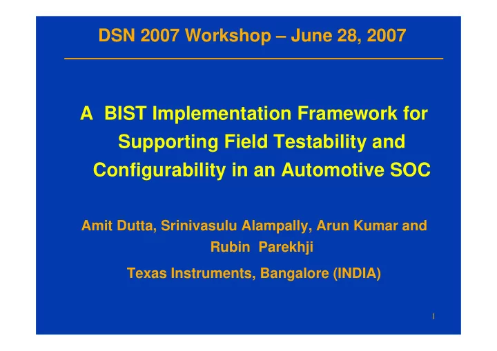
DSN 2007 Workshop June 28, 2007 A BIST Implementation Framework for Supporting Field Testability and Configurability in an Automotive SOC Amit Dutta, Srinivasulu Alampally, Arun Kumar and Rubin Parekhji Texas Instruments, Bangalore
DSN 2007 Workshop – June 28, 2007 A BIST Implementation Framework for Supporting Field Testability and Configurability in an Automotive SOC Amit Dutta, Srinivasulu Alampally, Arun Kumar and Rubin Parekhji Texas Instruments, Bangalore (INDIA) 1
Motivation Automotive chips require: � Field testability and low system DPPM. � Support / Reconfigurability for graceful degradation / diagnosis. Conventional BIST must be augmented to: � Provide high / selectable coverage. � Take corrective measures through self-analysis and self-repair. � Support for system and application level interfaces. Different high performance SOCs being designed in TI India with these requirements. 2
Presentation Outline � Requirements of manufacturing and field test. � Overview of techniques. Applicable scope. � System level requirements for self-test. � Logic self-test architecture and implementation. � Memory self-test and self-repair. � Device configuration. � Conclusion. 3
Why BIST? What Else? BIST widely used due to: � Test time / Test cost improvements. � Test quality improvements. Field testability. � Reduction in chip test resources / tester infrastructure. Difficulties due to: � Low coverage. � Design intrusive implementation (timing, bounding, test points). � Poor debug / diagnosis. 4
Why BIST? What Else? (2) One-time manufacturing test increasingly inadequate: � Need for periodic testing on field. � Need for conformance checks for operating parameters. � Insufficient screening with time zero tests. Solutions available: � Online testing, e.g. compute time redundancy. � Error correction, e.g. code space redundancy. � Fault tolerance, e.g. module redundancy. Impact in terms of design overhead, fault coverage and error detection latency. 5
Scope of System Test � Covered faults: static / parametric. � Test initiation: periodic / startup time. � Test operation: online interleaved / offline. � Test schedule: atomic / halt and resume. � Test configuration: fixed / selectable. � Test control: internal / tester interface / external. � Test granularity: modular / entire chip. � Test storage: RAM / ROM / Flash. � Device state: destroyed / restored. 6
System Test Requirements Enhancements to chip level BIST for system level test: � Trigger mechanisms: Through test modes / application firmware running on CPU. � Test configuration and interface: Through device internal test bus / external standard test / functional interface. � Test control for various configurations. � End of test status check and actions. � Specific requirements for device and application / system test. 7
System Level Self-test External host Read Master CPU or interface Self-test microcode Internal memory DUT (self-test config.) Write BIST - Status (Logic / Memory) registers 8
Design Considerations for Logic Self-test � X tolerance / X handling – Functional and timing. � Control of configuration and status registers. Test access protection. Test timeout – watchdog. � Internal clock control for high speed shift and at-speed capture. � I/O pad control for quiescent system interface. � Self-test control, indication and status. 9
Example: Internal Clock Control Capture Pulses Clock Dom 1 Clock Dom2 Skew ed Aligned Capt ure Last Shift Pulse Pulse Clock dom 1 Scan-en dom 1 Clock dom 2 Scan-en dom 2 Ctrl clock last last shift -1 shift 10
Self-test Architecture Deterministic BIST (DBIST) with re-seeding is used. Modifications required to support self-test include: � Internal re-seeding mechanism. � Memory mapping, DUT - DBIST interface, DBIST – test interface control. � Support for self-test: Pattern counter. Shift counter. � Clock control: Device internal shift and capture. � Internal signature storage and comparison. 11
Deterministic BIST Architecture 12
Logic BIST / Self-test Modules S/W mode write I/F BIST Progress Watchdog Configuration Tracker Timer Register File JTAG mode write I/F S/W mode read I/F Master Status Controller Register file JTAG mode read I/F BIST Protocol Read-Write Test mode Hard Macros Driver Controller controller ATE I/F Read I/F BIST Shadow Memory interface BIST Controller RAM Reg & PRPG Unit JTAG mode write I/F S/W mode write I/F DESIGN UNDER TEST Golden MISR Compare MISR Unit 13
Procedure for Self-test Reset deactivation Internal CPU Pulse activation Internal reset Set “DONE” Status to ‘1’ External host or YES CPU interface Control by NO 0 1 Seed count =0 BOOTSTRAP Execute functional Check self-test instruction completion set YES Compare golden MISR to ‘1’ NO YES Load self-test S/W NO Pattern count =0 Into internal RAM Execute self-test DBIST run routine 14
BIST and BISR for Memories � BIST for conventional reasons. � Programmable BIST: � For post-silicon encoding of (new) memory test algorithms. � Support for non-functional sequences, e.g. single cycle access, back-to-back accesses, accessing groups of memory banks together. � Online repair: � Reduction in test data volume. � Efficient analysis and allocation of spare resources. � Reconfiguration (leading to graceful degradation). � Implementation: Destructive test. Soft repair only. One memory type considered. 15
Design Considerations for Memory Test � Memory BIST activation mechanisms. � Memory grouping for test. State of CPU and L1 / L2 caches. � Fail data capture and analysis on chip: Tradeoffs in hardware overhead, analysis time, quality of repair solution. � Shifting new repair solution into memory address E-Fuse farm. � Resumption of next phase of memory test after completion of earlier phase of repair. 16
Memory Test / Repair Architecture PBIST controller CPU Memory under test Datalog register MMR space E-Fuse BISR Initial Data repair solution analyzer solution BISR shift clock 17
Procedure for Memory Test / Repair CPU S/W for memory test algorithm Memory set complete PBIST run PBIST Done No Failure ? Yes Shift repair Halt PBIST solution Log fail data Yes Analyze data No New solution Repairable? Abort 18
Device Overview � 2 IP cores and several other peripheral modules. � Multiple clocks and frequencies. Peak 450 MHz operation. PLL / clock TI 64x ARM 9x / test mode DSP core controller Bus protocol manager Memory BIST Self-test Peripheral Memory controller controller interfaces 19
Status and Summary � BIST and BISR implemented with different variations. � Silicon validation complete. � Methodology being replicated on other chips. � Firmware development in progress. � Scope extensions: � Status restoration. � Functional and structural tests. � Profiling for reliability DPPM. � “Online coverage of used logic” versus “Periodic coverage of all logic”. � Fault / Error tolerance. 20
Recommend
More recommend
Explore More Topics
Stay informed with curated content and fresh updates.
