UMBC A B M A L T F O U M B C I M Y O R T 1 - PowerPoint PPT Presentation
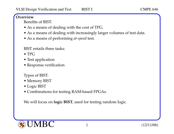
VLSI Design Verification and Test BIST I CMPE 646 Overview Benefits of BIST: As a means of dealing with the cost of TPG. As a means of dealing with increasingly larger volumes of test data. As a means of performing at-speed test.
VLSI Design Verification and Test BIST I CMPE 646 Overview Benefits of BIST: • As a means of dealing with the cost of TPG. • As a means of dealing with increasingly larger volumes of test data. • As a means of performing at-speed test. BIST entails three tasks: • TPG • Test application • Response verification Types of BIST: • Memory BIST • Logic BIST • Combinations for testing RAM-based FPGAs. We will focus on logic BIST , used for testing random logic. L A N R Y D UMBC A B M A L T F O U M B C I M Y O R T 1 (12/11/06) I E S R C E O V U I N N U T Y 1 6 9 6
VLSI Design Verification and Test BIST I CMPE 646 Overview Logic BIST uses pseudorandom ( PR ) tests, generated using a Linear Feedback Shift Register ( LFSR ) or cellular automata. Usually much longer than deterministic tests but much less costly to gener- ate. The large volume of data usually requires some sort of compactor to com- press the responses. There are several types but signature analyzers are the most popular. Test Controller Test Generator Response Verification CUT All components are on-chip. The controller manages the application of the test. L A N R Y D UMBC A B M A L T F O U M B C I M Y O R T 2 (12/11/06) I E S R C E O V U I N N U T Y 1 6 9 6
VLSI Design Verification and Test BIST I CMPE 646 PseudoRandom TPG and LFSRs PseudoRandom ( PR ) implies random patterns without repetition . Y 0 D Q D Q D Q (a) The number of Clk Clk Clk unique patterns Y 2 Y 3 is equal to the Y 1 The clock number of states is the only in the circuit. Y 0 (b) D Q D Q D Q input This is determined by Clk Clk Clk Autonomous the number and Y 2 Y 3 Y 1 LFSR position of the feedback tabs. Y 0 (c) D Q D Q D Q Clk Clk Clk Y 2 Y 3 Y 1 L A N R Y D UMBC A B M A L T F O U M B C I M Y O R T 3 (12/11/06) I E S R C E O V U I N N U T Y 1 6 9 6
VLSI Design Verification and Test BIST I CMPE 646 LFSRs For (a), the parity of the feedback tabs defines the input, Y 0 . ⊕ Y 0 Y 1 Y 3 = Let y 0 y 1 y 2 represent the present state of the registers and Y 1 Y 2 Y 3 represent the next state , then Y 1 = y 0 , Y 2 = y 1 and Y 3 = y 2 . Clk y 0 Y 1 Y 2 Y 3 Clk y 0 Y 1 Y 2 Y 3 Clk y 0 Y 1 Y 2 Y 3 1 0 0 1 1 0 0 1 1 0 0 1 1 1 1 0 0 1 0 1 0 0 1 1 1 0 0 2 1 1 1 0 2 0 0 1 0 2 0 1 1 0 3 0 1 1 1 3 1 0 0 1 3 0 0 1 1 4 1 0 1 1 4 1 0 0 1 5 0 1 0 1 6 0 0 1 0 7 1 0 0 1 The leftmost (a) LFSR was arbitrarily initialized to 001 . Generating 000 is not possible (the last row is identical to the first row). The maximal cycle of the LFSR is 7: (2 3 - 1). L A N R Y D UMBC A B M A L T F O U M B C I M Y O R T 4 (12/11/06) I E S R C E O V U I N N U T Y 1 6 9 6
VLSI Design Verification and Test BIST I CMPE 646 LFSRs Note that the relationship between the maximal cycle and the # of feedback tabs is not linear. Example (c) has 3 feedback tabs but can only generate 4 patterns. Adding a NOR as shown allows the all-zero pattern. zero Assume start state is: y 0 Y 1 Y 2 Y 3 =001. D Q D Q D Q Clk Clk Clk Y 2 Y 1 Y 3 y 0 Y 1 Y 2 Y 3 Clk zero 1 1 1 0 0 0 2 1 0 1 0 0 3 1 0 1 1 0 4 0 0 1 1 1 5 1 0 0 1 1 6 0 0 1 0 1 7 0 0 0 1 0 8 0 1 0 0 1 L A N R Y D UMBC A B M A L T F O U M B C I M Y O R T 5 (12/11/06) I E S R C E O V U I N N U T Y 1 6 9 6
VLSI Design Verification and Test BIST I CMPE 646 LFSR Configurations Two configurations: + + + Standard C 1 C 2 C N-1 C N D Q D Q D Q Clk Clk Clk C N C 1 C 2 C N-1 Modular + + + D Q D Q D Q Clk Clk Clk Note, there is only a tap and an XOR gate if C i =1. L A N R Y D UMBC A B M A L T F O U M B C I M Y O R T 6 (12/11/06) I E S R C E O V U I N N U T Y 1 6 9 6
VLSI Design Verification and Test BIST I CMPE 646 LFSR Configuration Examples This LFSR is equivalent to the version given in (a) previously. Modular version D Q D Q D Q (a) Clk Clk Clk Y 2 Y 3 Y 1 LFSRs that implements polynomial 1 + X 3 + X 4 . + X 2 X 3 X 4 1 X Standard D Q D Q D Q D Q Clk Clk Clk Clk Modular X 4 X 2 X 3 1 X + D Q D Q D Q D Q Clk Clk Clk Clk L A N R Y D UMBC A B M A L T F O U M B C I M Y O R T 7 (12/11/06) I E S R C E O V U I N N U T Y 1 6 9 6
VLSI Design Verification and Test BIST I CMPE 646 Analytical Framework for LFSRs The truth table for the XOR gate indicates it performs addition and subtraction , modulo 2. a b a XOR b a+b (sum) a-b (diff) a+b (carry) a-b (borrow) 0 0 0 0 0 0 0 0 1 1 1 1 0 1 1 0 1 1 1 0 0 1 1 0 0 0 1 0 Note that carry and borrow are not implemented because of the modulo 2. Expressing the output, Y j , as a function of time: ( ) ( ) ≠ for j Y j t Y j t = – 1 0 – 1 As a function of Y 0 , using X j as a translation operator: ( ) ( ) Y j t Y 0 t j = – ( ) X j ( ) Y j t Y 0 t = L A N R Y D UMBC A B M A L T F O U M B C I M Y O R T 8 (12/11/06) I E S R C E O V U I N N U T Y 1 6 9 6
VLSI Design Verification and Test BIST I CMPE 646 Analytical Framework for LFSRs In the standard form, Y 0 is the sum of other states as given by: N ∑ ( ) ( ) Y 0 t C j Y j t = Here, sum is XOR. j = 1 Substituting: N ( ) X j ∑ ( ) Y 0 t C j Y 0 t Eliminate Y j s. = j = 1 N C j X j ∑ ( ) ( ) Y 0 t Y 0 t = j = 1 N C j X j ∑ ( ) Y 0 t + 1 = 0 j = 1 ( ) P N X ( ) Y 0 t = 0 where P N (X) is called the characteristic polynomial L A N R Y D UMBC A B M A L T F O U M B C I M Y O R T 9 (12/11/06) I E S R C E O V U I N N U T Y 1 6 9 6
VLSI Design Verification and Test BIST I CMPE 646 Analytical Framework for LFSRs Assuming ( ) P N X ( ) ≠ Y 0 t then = 0 0 where N C j X j ∑ ( ) P N X = 1 + j = 1 The characteristic polynomials for (a), (b) and (c) given earlier are: •C 1 =1, C 2 =0, and C 3 =1 yields P 3 (X) = 1 + X + X 3 •C 1 =0, C 2 =0, and C 3 =1 yields P 3 (X) = 1 + X 3 •C 1 =1, C 2 =1, and C 3 =1 yields P 3 (X) = 1 +X +X 2 + X 3 The length of the LFSR sequence is determined by its characteristic polyno- mial. Only a primitive polynomial guarantees a maximal-length sequence of 2 N - 1. L A N R Y D UMBC A B M A L T F O U M B C I M Y O R T 10 (12/11/06) I E S R C E O V U I N N U T Y 1 6 9 6
VLSI Design Verification and Test BIST I CMPE 646 Operations on Polynomials Multiplication uses modulo 2 addition, e.g., x i + x i = 0. Division will be useful in response compaction. x 2 x 4 x 3 x + + 1 + + + 1 x 2 x x 4 x 3 + 1 + 1 + + + 1 x 4 2 x 4 x 3 x + + + + + 1 Multiplication x 5 x 4 x + + + x 3 x 2 + + + 1 x 5 x 3 x 3 Division x x + + + + 1 + + x 2 x + + 1 x 2 + + 1 x Irreducible polynomial properties : Cannot be factored, is divisible only by itself and 1, has a odd number of terms (including 1), is primitive if smallest k even divisible into 1 + x k is k = 2 N -1 (with N the degree of the polynomial). L A N R Y D UMBC A B M A L T F O U M B C I M Y O R T 11 (12/11/06) I E S R C E O V U I N N U T Y 1 6 9 6
VLSI Design Verification and Test BIST I CMPE 646 Primitive Polynomials All polynomials of degree 3 that include the 1 term: x 3 (a) + 1 = 0 x 3 x 2 (b) + + 1 = 0 x 3 x (c) + + 1 = 0 x 3 x 2 x (d) + + + 1 = 0 (b) and (c) are primitive, e.g., they divide evenly into x 7 - 1. (a) and (d) are reducible, e.g., x 3 + 1 = (x + 1)(x 2 + x + 1). The configuration of the LFSR introduces autocorrelation between consecu- tive sequences, e.g.,column for Y 2 and Y 3 from left side of slide 4 gave: (0011101)0 (1001110)1 Y 3 is 1 bit shifted to the right compared to Y 2 . This makes it difficult to detect some faults ( Random Pattern Resistant ( RPR )). L A N R Y D UMBC A B M A L T F O U M B C I M Y O R T 12 (12/11/06) I E S R C E O V U I N N U T Y 1 6 9 6
VLSI Design Verification and Test BIST I CMPE 646 Response Compaction The response of the logic-under-test needs to be checked after test application with an LFSR. It is difficult to check the response of every pattern (storage requirements). Instead, the responses are compressed and the compressed response is checked. The type of compression used here typically losses information and allows aliasing (identical faulty and fault-free circuit responses). The probability of aliasing decreases as the length of the test increases . There are several compaction testing techniques: • Parity testing • One counting • Transition counting • Syndrome calculation • Signature analysis L A N R Y D UMBC A B M A L T F O U M B C I M Y O R T 13 (12/11/06) I E S R C E O V U I N N U T Y 1 6 9 6
Recommend
More recommend
Explore More Topics
Stay informed with curated content and fresh updates.


