Built-In Self- Test (BIST) Virendra Singh Associate Professor C - PowerPoint PPT Presentation
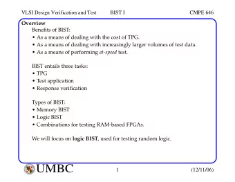
Built-In Self- Test (BIST) Virendra Singh Associate Professor C omputer A rchitecture and D ependable S ystems L ab Department of Electrical Engineering Indian Institute of Technology Bombay http://www.ee.iitb.ac.in/~viren/ E-mail:
Built-In Self- Test (BIST) Virendra Singh Associate Professor C omputer A rchitecture and D ependable S ystems L ab Department of Electrical Engineering Indian Institute of Technology Bombay http://www.ee.iitb.ac.in/~viren/ E-mail: viren@ee.iitb.ac.in EE-709: Testing & Verification of VLSI Circuits Lecture 33 (08 April 2013) CADSL
BIST Architecture Note: BIST cannot test wires and transistors: From PI pins to Input MUX From POs to output pins CADSL 08 Apr 2013 EE-709@IITB 2
Pattern Generation Store in ROM – too expensive Exhaustive Pseudo-exhaustive Pseudo-random (LFSR) – Preferred method Binary counters – use more hardware than LFSR Modified counters Test pattern augmentation LFSR combined with a few patterns in ROM Hardware diffracter – generates pattern cluster in neighborhood of pattern stored in CADSL 08 Apr 2013 EE-709@IITB 3 ROM
Pseudo-Random Pattern Generation Standard Linear Feedback Shift Register (LFSR) Produces patterns algorithmically – repeatable Has most of desirable random # properties Need not cover all 2 n input combinations Long sequences needed for good fault coverage CADSL 08 Apr 2013 EE-709@IITB 4
Matrix Equation for Standard LFSR 0 0 … 0 0 1 X 0 ( t ) X 0 ( t + 1) 0 1 … 0 0 0 . . . . . X 1 ( t ) X 1 ( t + 1) . . . . . . . . . . . . = . . 0 0 … 1 0 0 . . 0 0 … 0 1 0 X n -3 ( t ) X n -3 ( t + 1) 1 … h 2 h n -2 h n -1 h 1 X n -2 ( t ) X n -2 ( t + 1) X n -1 ( t ) X n -1 ( t + 1) X ( t + 1) = T s X ( t ) ( T s is companion matrix ) CADSL 08 Apr 2013 EE-709@IITB 5
Response Compaction Severe amounts of data in CUT response to LFSR patterns – example: Generate 5 million random patterns CUT has 200 outputs Leads to: 5 million x 200 = 1 billion bits response Uneconomical to store and check all of these responses on chip Responses must be compacted CADSL 08 Apr 2013 EE-709@IITB 6
Definitions Aliasing – Due to information loss, signatures of good and some bad machines match Compaction – Drastically reduce # bits in original circuit response – lose information Compression – Reduce # bits in original circuit response – no information loss – fully invertible (can get back original response) Signature analysis – Compact good machine response into good machine signature . Actual signature generated during testing, and compared with good machine signature Transition Count Response Compaction – Count # transitions from 0 1 and 1 0 as a signature CADSL 08 Apr 2013 EE-709@IITB 7
1’s Count Signature 3 4 3 4 3 2 CADSL 08 Apr 2013 EE-709@IITB 8
Transition Counting Transition count: m ⊕ C ( R ) = Σ ( r i r i -1 ) for all m primary outputs i = 1 To maximize fault coverage: Make C ( R 0) – good machine transition count – as large or as small as possible CADSL 08 Apr 2013 EE-709@IITB 9
Transition Counting CADSL 08 Apr 2013 EE-709@IITB 10
LFSR for Response Compaction • Use cyclic redundancy check code (CRCC) generator (LFSR) for response compacter • Treat data bits from circuit POs to be compacted as a decreasing order coefficient polynomial • CRCC divides the PO polynomial by its characteristic polynomial Leaves remainder of division in LFSR Must initialize LFSR to seed value (usually 0) before testing • After testing – compare signature in LFSR to known good machine signature • Critical: Must compute good machine signature CADSL 08 Apr 2013 EE-709@IITB 11
Example Modular LFSR Response Compacter • LFSR seed value is “00000” CADSL 08 Apr 2013 EE-709@IITB 12
Polynomial Division Inputs X 0 X 1 X 2 X 3 X 4 Initial State 0 0 0 0 0 1 1 0 0 0 0 0 0 1 0 0 0 0 Logic 0 0 1 0 0 0 Simulation: 0 0 0 1 0 1 1 0 0 0 1 0 1 0 0 1 0 1 1 1 0 0 1 0 1 0 1 1 0 Logic simulation: Remainder = 1 + x 2 + x 3 0 1 0 1 0 0 0 1 . . . . . . . . 0 x 0 + 1 x 1 + 0 x 2 + 1 x 3 + 0 x 4 + 0 x 5 + 0 x 6 + 1 x 7 CADSL 08 Apr 2013 EE-709@IITB 13
Symbolic Polynomial Division + 1 x 2 x 5 + x 3 + x + 1 + x + x 3 x 7 + x 2 + x 5 + x 3 x 7 + x + x 2 x 5 + x + 1 remainder + x 3 x 5 + 1 + x 2 x 3 Remainder matches that from logic simulation of the response compacter! CADSL 08 Apr 2013 EE-709@IITB 14
Multiple-Input Signature Register (MISR) • Problem with ordinary LFSR response compacter: Too much hardware if one of these is put on each primary output (PO) • Solution: MISR – compacts all outputs into one LFSR Works because LFSR is linear – obeys superposition principle Superimpose all responses in one LFSR – final remainder is XOR sum of remainders of polynomial divisions of each PO by the CADSL characteristic polynomial 08 Apr 2013 EE-709@IITB 15
MISR Matrix Equation • d i ( t ) – output response on PO i at time t 0 1 … 0 0 X 0 ( t + 1) X 0 ( t ) d 0 ( t ) 0 0 … 0 0 . . . . X 1 ( t + 1) X 1 ( t ) d 1 ( t ) . . . . . . . . . . . . . . = 0 0 … 1 0 . . + . 0 0 … 0 1 X n -3 ( t + 1) X n -3 ( t ) d n -3 ( t ) … 1 h 1 h n -2 h n -1 X n -2 ( t + 1) X n -2 ( t ) d n -2 ( t ) X n -1 ( t + 1) X n -1 ( t ) d n -1 ( t ) CADSL 08 Apr 2013 EE-709@IITB 16
Modular MISR Example 0 0 1 X 0 ( t + 1) X 0 ( t ) d 0 ( t ) = 1 0 1 + X 1 ( t + 1) X 1 ( t ) d 1 ( t ) 0 1 0 X 2 ( t + 1) X 2 ( t ) d 2 ( t ) CADSL 08 Apr 2013 EE-709@IITB 17
Multiple Signature Checking • Use 2 different testing epochs: 1 st with MISR with 1 polynomial 2 nd with MISR with different polynomial • Reduces probability of aliasing – Very unlikely that both polynomials will alias for the same fault • Low hardware cost: A few XOR gates for the 2 nd MISR polynomial A 2-1 MUX to select between two feedback polynomials CADSL 08 Apr 2013 EE-709@IITB 18
Aliasing Probability • Aliasing – when bad machine signature equals good machine signature • Consider error vector e ( n ) at POs Set to a 1 when good and faulty machines differ at the PO at time t ≡ • P al aliasing probability ≡ • p probability of 1 in e ( n ) • Aliasing limits: ≤ ≤ ≤ 0 < p ½, p k P al (1 – p ) k ≤ ≤ ≤ ≤ ½ p 1, (1 – p ) k P al p k CADSL 08 Apr 2013 EE-709@IITB 19
Aliasing Theorems • Theorem : Assuming that each PO d ij has probability p j of being in error, where the p j probabilities are independent, and that all outputs d ij are independent, in a k -bit MISR, P al = 1/(2 k ), regardless of the initial condition. CADSL 08 Apr 2013 EE-709@IITB 21
Transition Counting vs. LFSR • LFSR aliases for f sa1, transition counter for a sa1 Responses Pattern Good f sa1 b sa1 abc a sa1 0 1 0 0 000 1 1 0 1 001 0 1 0 1 010 0 1 0 1 011 0 1 1 0 100 1 1 1 1 101 1 1 1 1 110 1 1 1 1 111 Signatures 3 0 1 3 Transition Count 001 001 010 LFSR 101 CADSL 08 Apr 2013 EE-709@IITB 22
Logic BIST • Complex systems with multiple chips demand elaborate logic BIST architectures BILBO and test / clock system Shorter test length, more BIST hardware STUMPS & test / scan systems Longer test length, less BIST hardware • Benefits: cheaper system test, Cost: more hdwe. • Must modify fully synthesized circuit for BIST to boost fault coverage Initialization, loop-back , test point hardware CADSL 08 Apr 2013 EE-709@IITB 23
Test / Clock System Example • New fault set tested every clock period • Shortest possible pattern length 10 million BIST vectors, 200 MHz test / clock Test Time = 10,000,000 / 200 x 10 6 = 0.05 s Shorter fault simulation time than test / scan CADSL 08 Apr 2013 EE-709@IITB 24
BILBO – Works as PG and RC Built-in Logic Block Observer (BILBO) -- 4 modes: 1. Flip-flop 2. LFSR pattern generator 3. LFSR response compacter 4. Scan chain for flip-flops CADSL 08 Apr 2013 EE-709@IITB 25
Complex BIST Architecture • Testing epoch I: LFSR1 generates tests for CUT1 and CUT2 BILBO2 (LFSR3) compacts CUT1 (CUT2) • Testing epoch II: BILBO2 generates test patterns for CUT3 LFSR3 compacts CUT3 response CADSL 08 Apr 2013 EE-709@IITB 26
Bus-Based BIST Architecture Self-test control broadcasts patterns to each CUT over bus – parallel pattern generation Awaits bus transactions showing CUT’s responses to the patterns: serialized compaction CADSL 08 Apr 2013 EE-709@IITB 27
Built-in Logic Block Observer (BILBO) • Combined functionality of D flip-flop, pattern generator , response compacter , & scan chain Reset all FFs to 0 by scanning in zeros CADSL 08 Apr 2013 EE-709@IITB 28
Example BILBO Usage SI – Scan In SO – Scan Out Characteristic polynomial : 1 + x + … + x n CUTs A and C: BILBO1 is MISR, BILBO2 is LFSR CUT B: BILBO1 is LFSR, BILBO2 is MISR CADSL 08 Apr 2013 EE-709@IITB 29
BILBO Serial Scan Mode B 1 B 2 = “00” Dark lines show enabled data paths CADSL 08 Apr 2013 EE-709@IITB 30
BILBO LFSR Pattern Generator Mode • B 1 B 2 = “01” CADSL 08 Apr 2013 EE-709@IITB 31
BILBO in D FF (Normal) Mode • B 1 B 2 = “10” CADSL 08 Apr 2013 EE-709@IITB 32
BILBO in MISR Mode • B 1 B 2 = “11” CADSL 08 Apr 2013 EE-709@IITB 33
Recommend
More recommend
Explore More Topics
Stay informed with curated content and fresh updates.
