14:332:231 DIGITAL LOGIC DESIGN Ivan Marsic, Rutgers University - PDF document
14:332:231 DIGITAL LOGIC DESIGN Ivan Marsic, Rutgers University Electrical & Computer Engineering Fall 2013 Lecture #5: Combinational Circuit Analysis Combinational Circuit Analysis Combinational circuit : Output depends only on the
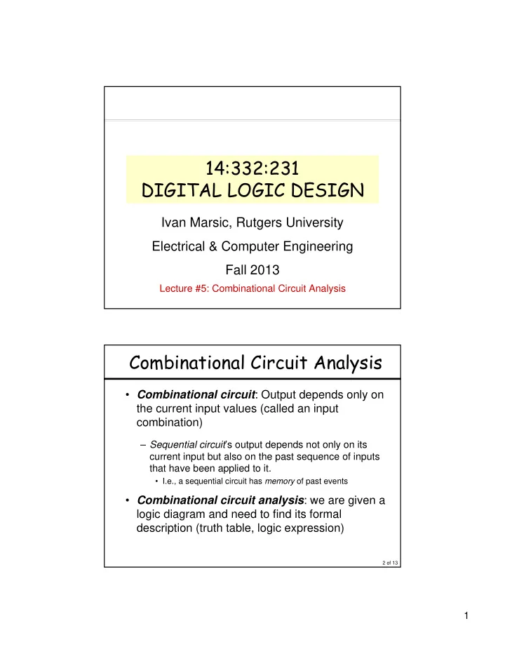
14:332:231 DIGITAL LOGIC DESIGN Ivan Marsic, Rutgers University Electrical & Computer Engineering Fall 2013 Lecture #5: Combinational Circuit Analysis Combinational Circuit Analysis • Combinational circuit : Output depends only on the current input values (called an input combination) – Sequential circuit ’s output depends not only on its current input but also on the past sequence of inputs that have been applied to it. • I.e., a sequential circuit has memory of past events • Combinational circuit analysis : we are given a logic diagram and need to find its formal description (truth table, logic expression) 2 of 13 1
Kinds of Combinational Analysis • Exhaustive (truth table) • Algebraic (expressions) • Simulation / test bench (in the laboratory) 3 of 13 Exhaustive — Truth Table X Given: Y Z F Find truth table by all input combinations: 00001111 00001111 X 11001111 00110011 Y 01000101 11001100 01010101 01010101 Z 01100101 F 11110000 00110011 00100000 10101010 4 of 13 2
Exhaustive — Truth Table 00001111 00001111 X 11001111 00110011 Y 01000101 11001100 01010101 01010101 Z 01100101 F 11110000 00110011 00100000 10101010 Row X Y Z F 0 0 0 0 0 1 0 0 1 1 2 0 1 0 1 3 0 1 1 0 4 1 0 0 0 Find truth table by all input combinations: 5 1 0 1 1 6 1 1 0 0 7 1 1 1 1 5 of 13 Algebraic — Signal Expressions X+Y X (X+Y ) Z Y F = ((X+Y ) Z) + (X Y Z ) Y Z X X Y Z Z Use theorems to transform F into another form E.g., “multiplying out”: F = ((X+Y ) Z) + (X Y Z ) = (X Z) + (Y Z) + (X Y Z ) … 6 of 13 3
Algebraic — Signal Expressions …and obtain a new circuit but the same function: X X+Y Y F = ((X+Y ) Z) + (X Y Z ) Y Z Y Z X X Y Z Z Two-level AND-OR circuit 7 of 13 “Add out” Logic Function “Add out” logic function is OR-AND circuit: F = ((X + Y ) Z) + (X Y Z ) two-level AND-OR circuit = (X + Y + X ) (X + Y + Y) (X + Y + Z ) (Z + X ) (Z + Y) (Z + Z ) = 1 1 (X + Y + Z ) (X + Z) (Y + Z) 1 = (X + Y + Z ) (X + Z) (Y + Z) two-level OR-AND circuit Two-level OR-AND circuit: X Y X+Y +Z Z F = (X+Y +Z ) (X +Z) (Y+Z) X +Z X Y+Z Y Z 8 of 13 4
Another Example G(W, X, Y, Z) = W X Y + Y Z (W X Y) W X Y W W X X G G (Y Z) Y Z Y Y Z Z two-level AND-OR two-level NAND-NAND (W X) W W X Y X Y G Y Z Y Z with 2-input gates only 9 of 13 Yet Another Example (1) W (W X ) using NAND and NOR gates: X ((W X ) Y) X Y W F (W +X+Y ) = [ ((W X ) Y) + (W +X+Y ) + (W+Z) ] Y (W+Z) Z 10 of 13 5
[ RECALL from Lecture #4 ] DeMorgan Symbols X Y (X Y ) OR (X Y) X Y NOR X Y (X + Y ) AND (X Y) X + Y NAND (X ) X BUFFER X X INVERTER 11 of 13 Yet Another Example (1) W (W X ) using NAND and NOR gates: X ((W X ) Y) X Y W F (W +X+Y ) = [ ((W X ) Y) + (W +X+Y ) + (W+Z) ] Y (W+Z) Z W W +X after substitution of some X ((W +X) Y) X NAND and NOR gates: Y W (W +Y+Y ) F =((W +X) Y) (W +X+Y ) (W+Z) Y (W+Z) …same function, according to Z the generalized DeMorgan’s theorem 12 of 13 6
Yet Another Example (2) bubble-to-bubble: different circuit but the same function: W W +X X (W +X) Y X Y W W +X+Y F Y =((W +X) Y) (W +X+Y ) (W+Z) W+Z Z here, majority are AND and OR gates 13 of 13 7
Recommend
More recommend
Explore More Topics
Stay informed with curated content and fresh updates.
