Hardware Design with VHDL Sequential Circuit Design I ECE 443 - PowerPoint PPT Presentation
Hardware Design with VHDL Sequential Circuit Design I ECE 443 Sequential Circuit Design: Principle Outline: Overview of sequential circuits Synchronous circuits Danger of synthesizing asynchronous circuit Inference of basic
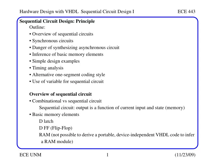
Hardware Design with VHDL Sequential Circuit Design I ECE 443 Sequential Circuit Design: Principle Outline: • Overview of sequential circuits • Synchronous circuits • Danger of synthesizing asynchronous circuit • Inference of basic memory elements • Simple design examples • Timing analysis • Alternative one-segment coding style • Use of variable for sequential circuit Overview of sequential circuit • Combinational vs sequential circuit Sequential circuit: output is a function of current input and state (memory) • Basic memory elements D latch D FF (Flip-Flop) RAM (not possible to derive a portable, device-independent VHDL code to infer a RAM module) ECE UNM 1 (11/23/09)
Hardware Design with VHDL Sequential Circuit Design I ECE 443 D Latch D latch is a level sensitive memory element, while the D flip-flop (FF) is an edge sensitive memory element Note that for the D latch, next state q* is d when the control signal c (often clock) is high, while q* is q when c is low ECE UNM 2 (11/23/09)
Hardware Design with VHDL Sequential Circuit Design I ECE 443 D Latch Timing diagram for D-latch -- note that d is sampled and stored on falling edge of c . Since the latch is "transparent" when c is asserted, it may cause racing if a loop exists in the circuit Cannot be used to swap data because of loop Not often used in synthesis because of this ECE UNM 3 (11/23/09)
Hardware Design with VHDL Sequential Circuit Design I ECE 443 D Flip Flop (FF) The D FF is only activated when the clk signal changes from 0 to 1. Activation implies it samples the value on its d input, stores the value in its memory and propagates the value to its output q ECE UNM 4 (11/23/09)
Hardware Design with VHDL Sequential Circuit Design I ECE 443 D Flip Flop (FF) D FF have advantages • glitches on d do not effect the state of the memory • The is no race condition -- swap circuits actually work D FF disadvantages • About twice as large as a D latch Timing behavior of a D FF: T hold T cq T setup • Clock-to-q delay (T cq ): Delay required for sampled d value to show up on q ECE UNM 5 (11/23/09)
Hardware Design with VHDL Sequential Circuit Design I ECE 443 D Flip Flop (FF) • Setup time (T setup ): time interval that d must be stable for before the rising edge of clock • Hole time (T hold ): time interval that d must be stable for after the rising edge. T hold T cq T setup T cq is corresponds to the propagation delay of a combinational circuit, while T setup and T hold are timing constraints -- d must be stable for a time interval around clk If d changes during this interval, a setup time or hold time violation occurs and the D FF may enter a metastable state ( q is neither a 0 or 1) ECE UNM 6 (11/23/09)
Hardware Design with VHDL Sequential Circuit Design I ECE 443 The Clock Signal The clock signal plays a key role in sequential circuit design Systems can be classified according to the clock signal arrangement Globally synchronous circuit All memory elements (D FFs) are controlled ( synchronized ) by a common glo- bal clock signal (most popular) Globally asynchronous but locally synchronous circuit (GALS) Used in cases in which the components of the design are spread too far apart to allow a single synchronous clock -- a globally asynchronous circuit results However, the smaller subsystems use a synchronous clock internally Special interface circuits needed between subsystems to ensure proper operation Globally asynchronous circuits No clock is used to coordinate the memory elements ECE UNM 7 (11/23/09)
Hardware Design with VHDL Sequential Circuit Design I ECE 443 The Clock Signal Globally asynchronous circuits There are two categories • Systems that do not use the clock in a disciplined manner, for example, a ripple counter : clock port of an FF is connected to the q output of previous FF Poor design and not recommended • Systems that contain ’clockless’ memory components such as the latch or a combinational circuit with feedback loops ( asynchronous circuit) Proper design is entirely different to synchronous circuits not recommended for HDL synthesis either Synchronous circuit State registers (state_reg) represent the memory elements Next state logic represent the combinational circuit that determines state_next ECE UNM 8 (11/23/09)
Hardware Design with VHDL Sequential Circuit Design I ECE 443 Synchronous Circuits Operation is as follows: • At the rising edge of the clock, state_next is sampled and stored into the register (and becomes the new value of state_reg ) • The external inputs and state_reg signals propagate through next-state and output logic to determines the new values of the state_next and output signals • At the rising edge of the clock, the new value of state_next is sampled and stored and the process repeats Note that the clock period needs to be large enough to accommodate the propagation delay of the next-state logic, the clock-to-q delay and the setup time of the FFs Advantages of synchronous design • A single global clock makes the task of satisfying the timing constraints of a design with of thousands of FFs manageable and doable • The synchronous model separates the combinational components from the memory elements, making it possible to treat the combinational part by itself • Propagation delay anomalies such as hazards can be dealt with easily by focusing on the worst case timing behavior ECE UNM 9 (11/23/09)
Hardware Design with VHDL Sequential Circuit Design I ECE 443 Synchronous Circuits Therefore, the synchronous model reduces a complex sequential circuit to a single closed feedback loop and greatly simplifies the design process Types of synchronous circuits • Regular sequential circuit State representation, transitions and next-state logic have a simple, regular pat- tern, as in a incrementor or shift register • Random sequential circuit (FSM) More complicated state transitions and no special relationship between states and their binary representations -- next-state logic is random • Combined sequential circuit (FSM with a Data path, FSMD -- RTL) Combines regular sequential circuit and an FSM, with FSM acting as control for the sequential circuit Danger of Synthesizing an Asynchronous Circuit Consider the D Latch described earlier We can write VHDL code as follows to represent it ECE UNM 10 (11/23/09)
Hardware Design with VHDL Sequential Circuit Design I ECE 443 Danger of Synthesizing an Asynchronous Circuit library ieee; use ieee.std_logic_1164. all ; entity dlatch is port ( c: in std_logic; d: in std_logic; q: out std_logic ); end dlatch; architecture demo_arch of dlatch is signal q_latch: std_logic; begin ECE UNM 11 (11/23/09)
Hardware Design with VHDL Sequential Circuit Design I ECE 443 Danger of Synthesizing an Asynchronous Circuit process (c, d, q_latch) begin if ( c=’1’ ) then q_latch <= d; else q_latch <= q_latch; end if ; end process ; q <= q_latch; end demo_arch; Synthesis software will recognize this as the code for a D latch and should infer a predesigned D-latch from the cell library But what if we try to synthesis it from scratch, using simple gates? ECE UNM 12 (11/23/09)
Hardware Design with VHDL Sequential Circuit Design I ECE 443 Danger of Synthesizing an Asynchronous Circuit Here we see the implementation is combinational except for that the output is looped around as an input Unfortunately, there is a serious timing problem with this circuit Assume all gates have a propagation delay of T and c , d and q are initially ’1’ What happens when c changes from ’1’ to ’0’ at time t 0 ? From the function table, q should be latched to the value of d (’1’) 1) At t 0 , c changes to ’0’ 2) At t 1 , (after delay T ), dc and cn change 3) At t 2 , (after delay 2T ), qcn changes (due to cn ) and q changes (due to dc ) 4) At t 3 , (after delay 3T), q changes (due to qcn ) and qcn Therefore, output q oscillates at period of 2T changes (due to q ) ECE UNM 13 (11/23/09)
Hardware Design with VHDL Sequential Circuit Design I ECE 443 Inference of Basic Memory Elements You should use the following ’templates’ to create latches and FFs, so that the prede- signed library cells are inferred by the synthesis tools. D Latch • Eliminate the else branch to create a latch library ieee; use ieee.std_logic_1164. all ; entity dlatch is port ( c: in std_logic; d: in std_logic; q: out std_logic ECE UNM 14 (11/23/09)
Hardware Design with VHDL Sequential Circuit Design I ECE 443 Inference of Basic Memory Elements ); end dlatch; architecture arch of dlatch is begin -- c and d in sens. list b/c process sens. to both process (c, d) begin if (c=’1’) then q <= d; end if ; end process ; end arch; Pos Edge-Triggered D FF • No else branch -- NOTE sensitivity list library ieee; use ieee.std_logic_1164. all ; ECE UNM 15 (11/23/09)
Hardware Design with VHDL Sequential Circuit Design I ECE 443 Inference of Basic Memory Elements entity dff is port ( clk: in std_logic; d: in std_logic; q: out std_logic ); end dff; architecture arch of dff is begin process (clk) -- d not needed b/c process does nothing begin -- when d changes (unlike latch) ECE UNM 16 (11/23/09)
Recommend
More recommend
Explore More Topics
Stay informed with curated content and fresh updates.
