spintronics Influence of spin Magnetic on conduction - PowerPoint PPT Presentation
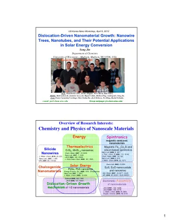
Albert Fert, UMR CNRS/Thales, Palaiseau, and Universit Paris-Sud, Orsay, France The origin, the development and the future of spintronics Influence of spin Magnetic on conduction nanostructures spin Spin up electron charge Spintronics
Albert Fert, UMR CNRS/Thales, Palaiseau, and Université Paris-Sud, Orsay, France The origin, the development and the future of spintronics Influence of spin Magnetic on conduction nanostructures spin Spin up electron charge Spintronics Spin down electron électron GMR, TMR, etc… Memory (M-RAM) Magnetic switching and microwave generation by spin transfer, spintronics with semiconductors, molecular spintronics , etc
Spin dependent conduction in ferromagnetic metals (two current model) n (E) Mott, Proc.Roy.Soc A153, 1936 E F Fert et al, PRL 21, 1190, 1968 Loegel-Gautier, JPCS 32, 1971 E Fert et al,J.Phys.F6, 849, 1976 Dorlejin et al, ibid F7, 23, 1977 I n (E) = / or I = ( - )/ ( + ) = ( - 1)/( + 1) 0.3 n (E) Cr d level E F Ni d band Virtual bound 20 state E Ni d band n (E) Cr d level Ti V Cr Mn Fe Co Ni
Mixing impurities A and B with opposite or similar spin asymmetries: the pre-concept of GMR Example: Ni + impurities A and B (Fert-Campbell, 1968, 1971) 1st case 2d = / A > 1, B < 1 A and B > 1 case High mobility channel low spin spin spin spin AB >> A + B AB A + B J. de Physique 32, 1971
Molecular Beam Epitaxy (growth of metallic multilayers)
• Magnetic multilayers Fe Cr Fe Cr Fe
• Magnetic multilayers Magnetizations of Fe layers at zero field in Fe/Cr multilayers Fe Cr Fe Cr Fe P. Grünberg, 1986 antiferromagnetic interlayer coupling
• Magnetic multilayers Magnetizations of H Fe layers in an applied field in Fe/Cr multilayers Fe Cr Fe Cr Fe P. Grünberg, 1986 antiferromagnetic interlayer coupling
• Giant Magnetoresistance (GMR) (Orsay, 1988, Fe/Cr multilayers, Jülich, 1989, Fe/Cr/Fe trilayers) Jülich Resistance ratio Orsay ~ + 80% V=RI Magnetic field (kGauss) Current AP (AntiParallel) P (Parallel)
• Giant Magnetoresistance (GMR) (Orsay, 1988, Fe/Cr multilayers, Jülich, 1989, Fe/Cr/Fe trilayers) Anti-parallel magnetizations (zero field, high resistance) Resistance ratio Fe Cr Fe ~ + 80% Parallel magnetizations (appl. field, low resist.) net Fe Magnetic field (kGauss) current Cr Fe Current AP (AntiParallel) P (Parallel) Condition for GMR: layer thickness nm
Read head of hard disc drive voltage current Magnetic fields generated by the media track 0 5 nm GMR sensor 1997 (before GMR) : 1 Gbit/in 2 , 2007 : GMR heads ~ 300 Gbit/in 2
Arrays of GMR biochips for analysis of biomolecules ( example: antigens are trapped by antibodies and also decorated by other antibodies labelled by magnetic nanoparticles which are detected by a GMR sensor) 9 m (Philips), 1 m (Santa Barbara) Probe arrays for analysis of thousands of different targets in parallel
• Magnetic Tunnel Junctions,Tunneling Magnetoresistance (TMR) 0.1 m ~ 100 nm tunneling ferromagnetic barrier electrodes AP (insulator) P Jullière, 1975, Low resistance state High resistance state low T, hardly Moodera et al, 1995, Miyasaki et al,1995, CoFe/Al 2 O 3 /Co, MR 30- reproducible 40% Applications: - read heads of Hard Disc Drive - M-RAM (Magnetic Random Access Memory) : density/speed of MRAM DRAM/SRAM + nonvolatilty + low energy consumption
Epitaxial magnetic tunnel junctions (MgO, etc) First examples on Fe/MgO/Fe(001): CNRS/Thales (Bowen, AF et al, APL2001) Nancy (Faure-Vincent et al, Yuasa et al, Fe/MgO/Fe APL 2003) Tsukuba (Yuasa et al, Nature Nature Mat. 2005 Mat. 2005) IBM (Parkin et al, Nature ΔR/R = (R AP -R P )/ R P 200% at RT Mat. 2005) ….etc Clearer picture of the CoFeB/MgO/CoFeB, 2006- physics of TMR : ΔR/R 500% at RT in several 2007 + what is inside the word laboratories in 2006-2007 « spin polarization »?
Mathon and Umerski, PR B 1999 1 Mavropoulos et al, PRL 2000 Butler P et al , PR B 2001 Zhang and Butler, PR B 2004 [bcc Co/MgO/bcc Co(001)] 2’ 5 1 AP 2’ 5
Zhang and Butler, PR B 2004 Beyond MgO MgO, ZnSe (Mavropoulos et al, PRL 2000), etc 1 1 symmetry (sp) slowly decaying P tunneling of Co majority spin 2’ 5 electrons SrTiO 3 and other d-bonded insulators (Velev et al , PRL 95, 2005; Bowen et al, PR B 2006) 5 symmetry (d) slowly decaying AP 1 tunneling of Co minority spin electrons 2’ 5 in agreement with the negative polarization of Co found in TMR with SrTiO 3 ,TiO 2 and Ce 1-x La x O 2 barriers (de Teresa, A.F. et al, Science 1999)
Zhang and Butler, PR B 2004 Beyond MgO MgO, ZnSe (Mavropoulos et al, PRL 2000), etc 1 P 1 symmetry (sp) slowly decaying tunneling of Co majority spin 2’ 5 electrons SrTiO 3 and other d-bonded insulators (Velev et al , PRL 95, 2005; Bowen et al, PR B 2006) 1 AP 5 symmetry (d) slowly decaying tunneling of Co minority spin electrons 2’ 5 in agreement with the negative Physical basis of « spin polarization of Co found in TMR with polarization »( SP ) SrTiO 3 ,TiO 2 and Ce 1-x La x O 2 barriers ¤Tunneling: SP of the DOS for the (de Teresa, A.F. et al, Science 1999) symmetry selected by the barrier ¤Electrical conduction: SP depends on scatterers, impurities ,..
Spin Transfer (magnetic switching, microwave generation) Spintronics with semiconductors Spintronics with molecules
Spin Transfer (magnetic switching, microwave generation) Spintronics with semiconductors Spintronics with molecules Introduction: spin accumulation and spin currents
Co/Cu: Current in Plane (CIP)-GMR ( Mosca, AF et al, JMMM 1991) CIP-GMR 6 nm scaling length = mean free path 60 nm 10 Co/Cu: Current to Plane (CPP) GMR 8 ( L.Piraux, AF et al, APL 1994,JMMM 1999) MR ratio (%) CPP-GMR 6 scaling length = spin diffusion 4 400 nm length >> mean free path 2 spin accumulation theory, (Valet-Fert, PR B 1993) 0 0 100 200 300 400 500 Co thickness (nm)
Spin injection/extraction at a NM/FM interface (beyond ballistic range) (illustration in the simplest NM FM case = flat band, low current, no interface resistance, zone of spin single polarity) accumulation FM l = spin diffusion length in FM sf NM FM l NM l l = spin diffusion length in NM sf sf sf (example: 0.5 m in Cu, >10 m in carbon E nanotube) E F = spin chemical potential Spin accumulation = E F -E F FM E F -E F ~ exp(z/ ) in FM l sf z NM E F -E F ~ exp(-z/ ) in NM l E F sf E F = spin chemical potential Spin current = J -J J -J FM NM l l = current spin polarization sf sf J +J z
Spin injection/extraction at a Semiconductor/FM interface NM = metal or FM semiconducto 1) situation without zone of spin r interface resistance accumulation (« conductivity mismatch ») FM NM l (Schmidt et al, PR B 2000) l sf sf E Semiconductor/ F metal E F Spin accumulation If similar spin spliting on both sides = E F -E F but much larger density of states in F metal z E F E F much larger spin accumulation density Spin current and much more spin flips NM= metal = J -J FM on magnetic metal side NM l l sf sf NM = z semiconductor almost complete depolarization of
Spin injection/extraction at a Semiconductor/FM interface spin dependent. interf. NM = FM resist. (ex:tunnel barrier) semiconducto e - r Spin dependent drop of the electro-chemical potential NM FM l l sf sf Discontinuity increases the z E F spin accumulation in NM E F re-balanced spin relaxations E F Spin accumulation in F and NM = E F -E F extension of the spin- E F polarized current into the Current Spin semiconductor Polarization * N r r l Rasbah, PR B 2000 b N N sf (J -J )/(J +J ) A.F-Jaffrès, PR B 2001
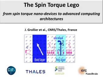
Spin transfer (J. Slonczewski, JMMM 1996, L. Berger, PR B 1996) Ex:Cobalt/Copper/ Cobalt S
Spin transfer (J. Slonczewski, JMMM 1996, L. Berger, PR B 1996) Ex:Cobalt/Copper/ Cobalt The transverse component of the spin current is absorbed and transferred to the total spin of the layer S j M x (M x M 0 ) Torque on S S Mx(MxM 0 )
Experiments on pillars Au Free ferro 4 nm Cu 10 nm a) First regime (low H): Fixe irreversible switching d I - Cu V - ferro (CIMS) Metallic pillar 50x150 nm² b) Second regime (high H): Au steady precession (microwave generation) Free ferro 4 nm barrier 10 nm Fixe d I - Cu V - ferro Tunnel junction E-beam lithography + etching
AP state Regime of irreversible magnetic switching of m First experiments on pillars: M Cornell (Katine et al, PRL 2000) m AP 0.1 CNRS/Thales (Grollier et al, APL 2001) 0.0 P M P state z IBM (Sun et al, APL 2002) -0.1 of m 1.0 -1.0 0.5 -0.5 0.0 0.0 -0.5 M 0.5 M y GaMnAs/InGaAs/GaMnAs x -1.0 1.0 Py/Cu/Py 50nmX150nm (Boulle, AF et al) tunnel junction (MR=150%) 1 4 , 6 (Elsen, AF et al, PR B 2006) H=7 Oe 30 K RT 55 000 0 ) d ( I 1 4 , 5 ( ) V / AP R e sistan ce 50 000 0 d P 45 000 0 1 4 , 4 - 2 0 40 000 0 I ( m A ) 5 4 4 5 0.0 -1.0x10 -5.0x10 5.0x10 1.0x10 Current density (A.cm -2 ) typical switching current 10 7 A/cm 2 switching time can be as short as 0.1 ns (Chappert et al) 1 x 10 5 A/cm 2
Recommend
More recommend
Explore More Topics
Stay informed with curated content and fresh updates.
