Spintronics material aspects Spintronics material aspects Why to - PowerPoint PPT Presentation
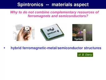
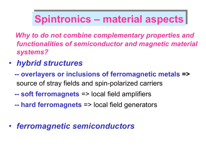
Spintronics material aspects Spintronics material aspects Why to do not combine complementary properties and functionalities of semiconductor and magnetic material systems? hybrid structures -- overlayers or inclusions of
Spintronics – material aspects Spintronics – material aspects Why to do not combine complementary properties and functionalities of semiconductor and magnetic material systems? • hybrid structures -- overlayers or inclusions of ferromagnetic metals => source of stray fields and spin-polarized carriers -- soft ferromagnets => local field amplifiers -- hard ferromagnets => local field generators • ferromagnetic semiconductors
MAGNETIC SEMICONDUCTORS MAGNETIC SEMICONDUCTORS Tomasz DIETL Institute of Physics, Polish Academy of Sciences, Warsaw Collaboration: Grenoble (J. Cibert et al.), Sendai (H. Ohno et al.), Austin (a. MacDonald et al.), Regensburg (D. Weiss et al.), … 1. Families of magnetic semiconductors 2. Spin manipulations in ferromagnetic semiconductors 3. Magnetic impurities in semiconductors 4. sp-d exchange interactions 5. d-d exchange interactions 6. Outlook 7. Summary Support: EC: AMORE, FENIKS, ERATO (JST), A.V. Humboldt Foundation
Families of magnetic semiconductors
Magnetic semiconductors Magnetic semiconductors • magnetic semiconductors short-range ferromagnetic super- or double exchange EuS, ZnCr 2 Se 4 , La 1-x Sr x MnO 3 , ... short-range antiferromagnetic superexchange EuTe, ...
now: Diluted Magnetic Semiconductors (DMS)
DMS: standard semiconductor + DMS: standard semiconductor + magnetic ions magnetic ions • Various magnetic ions: - mostly 3d transition metals: Sc, ..., Cu - rare earth (4f): Ce, ..., Tm - also actinides (5f), 4d TM, ... • Various hosts: - II-VI: Cd 1-x Mn x Te, Hg 1-x Fe x Se,... - IV-VI: Sn 1-x Mn x Te, Pb 1-x Eu x S - III-V: In 1-x Mn x Sb, Ga 1-x Er x N, ... - IV: Ge 1-x Mn x , Si 1-x Ce x - ....
Most of DMS: random antiferromagnet Most of DMS: random antiferromagnet short range antiferromagnetic superexchange
Evidences for antiferromagnetic pairs Evidences for antiferromagnetic pairs H 12 = - 2 J S 1 S 2 H 12 = - 2 J S 1 S 2 inelastic neutron scattering Zn 0.95 Mn 0.05 Te T. Giebultowicz et al. H. Kepa, …, T.D., PRL’03
Evidences for antiferromagnetic Evidences for antiferromagnetic interactions: magnetic susceptibility interactions: magnetic susceptibility Curie-Weiss law χ = C /( T − Θ ) C = g µ B S ( S +1) xN o /3 k B Θ < 0 antiferro A. Lewicki et al.
Magnetization of localized spins Magnetization of localized spins M(T,H) = g µ B Sx eff N o B S [ g µ B H / k B (T + T AF ) antiferromagnetic interactions x eff < x T AF > 0 Modified Brillouin function Y. Shapira et al.
Ferromagnetic DMS Ferromagnetic DMS long-range hole-mediated ferromagnetic exchange IV-VI: p-Pb 1-x-y Mn x Sn y Te (Story et al.’86) III-V: In 1-x- Mn x As (Ohno et al.’92) Ga 1-x- Mn x As (Ohno et al.’96) T C ≈ 100 K for x = 0.05 II-VI: p-Cd 1-x Mn x Te/Cd 1-x-y Zn x Mg y Te:N QW (Haury et al.’97, Kossacki et al.’99) p-Zn 1-x Mn x Te:N (Ferrand et al.’99) p-Be 1-x Mn x Te:N (Hansen et al.’01) III-V and II-VI DMS: quantum nanostructures and ferromagnetism combine
Spin manipulations in ferromagnetic DMS
Tuning magnetic ordering by Tuning magnetic ordering by electric field (ferro-FET) (In,Mn)As electric field (ferro-FET) (In,Mn)As M I V H H. Ohno, .., T.D., ...Nature ’00
Modulation-doped p-type magnetic QWs Modulation-doped p-type magnetic QWs (Cd,Mg)Te:N (Cd,Mg)Te:N (Cd,Mn)Te σ + σ - σ + σ - ENERGY ∆ E ~ M J. Cibert et al. (Grenoble)
Control of Control of V ferromagnetism ferromagnetism p doped by electric by electric QW field in a pin undoped field in a pin barriers diode – ferro-LED diode – ferro-LED n doped Photoluminescence a b 0V -1V 4.2 K 4.2 K PL Intensity (a.u.) 3.03 2.97 E c 2.82 2.80 2.19 2.19 E F 2.05 2.05 1.87 1.88 1.65 1.65 V 1.49 K 1.49 K E v 1700 1710 1700 1710 Hole liquid Depleted Energy (meV) H. Boukari, …, T.D., PRL’02
Combined: electrostatic Combined: electrostatic gate + illumination V gate + illumination in p-i-n diode (ferro-LED) in p-i-n diode (ferro-LED) QW a b 0V -1V 1.5 K 4.2 K 4.2 K 0 V PL Intensity (a.u.) 3.03 2.97 2.82 n 2.80 o 2.19 i 2.19 t a 2.05 n 2.05 i m 1.87 1.88 u 1.65 1.65 l l 1.49 K 1.49 K i 1700 1710 1700 1710 E c 1700 1710 Energy (meV) Hole liquid Depleted Ferro- diode: E F electric field and light tuned ferromagnetism V E v
Optical tuning of magnetization – p-i-p diode Optical tuning of magnetization – p-i-p diode paramagnetic E c p T × 10 10 p =16 × 10 10 cm -2 T = 1.34 K -2 Hole concentration cm 4.2 K 2.7 Temperature Illumination 2.7 K 5.2 2.4 K 7.1 2.1 K 10 E F 1.8 K 12 E v (a) (b) 1.2 K 16 1680 1690 1700 1710 1680 1690 1700 1710 CdMnTe QW Energy [ m eV ] Energy [ m eV ] 8 nm T = const p = const ferromagnetic 0 to 4% Mn pip diode: light destroys ferromagnetism
Magnetic ions in semiconductors • position of d levels, U • charge and spin states • intra ion excitation energies d � d* • coupling to band states: -- spin dependent: sp-d exchange interactions -- spin independent: band offsets -- crystal-field effects
Transition metals – free atoms Transition metals – free atoms • Electronic configuration of TM atoms: 3d n 4s 2 1 ≤ n ≤ 10: Sc, Ti, V, Cr, Mn, Fe, Co, Ni, Cu, Zn • Important role of electron correlation for open d shells - intra site correlation energy U = E n+1 – E n 3d 6 UHB for n =5, U ≈ 15 eV U LHB 3d 5
Transition metals – free atoms Transition metals – free atoms • Electronic configuration of TM atoms: 3d n 4s 2 1 ≤ n ≤ 10: Sc, Ti, V, Cr, Mn, Fe, Co, Ni, Cu, Zn • Important role of electron correlation for open d shells - intra site correlation energy U = E n+1 – E n for n =5, U ≈ 15 eV - intra-site exchange interaction: ferromagnetic Hund’s rule: S the highest possible for n = 5 , E S=3/2 − E S=5/2 ≈ 2 eV 3d * 5 3d 5
Transition metals – free atoms Transition metals – free atoms • Electronic configuration of TM atoms: 3d n 4s 2 1 ≤ n ≤ 10: Sc, Ti, V, Cr, Mn, Fe, Co, Ni, Cu, Zn • Important role of electron correlation for open d shells - intra site correlation energy U = E n+1 – E n for n =5, U ≈ 15 eV - intra-site exchange interaction: ferromagnetic Hund’s rule: S the highest possible for n = 5 , E S=3/2 − E S=5/2 ≈ 2 eV 4s 1 - TM atoms, 3d n 4s 1 , e.g., Mn : E S=2 − E S=3 ≈ 1.2 eV � J s-d ≈ 0.4 eV ferromagnetic despite of screening and hybridization these 3d 5 effects survive in solids
Where d levels and carriers reside in DMS? Where d levels and carriers reside in DMS? Possibilities: -- manganides La 1-x Sr x MnO 3 -- cuprates La 2-x Sr x CuO 4 Mott-Hubbard AF insulator for x � 0 charge transfer AF insulator for x � 0 E c.b. (cation s orbitals) c.b. d TM band v.b. v.b. (anion p orbitals) d TM band DOS Experimental guide: impurity limit (EPR, d –> d*, … )
TM impurities in II-VI compounds TM impurities in II-VI compounds • TM atoms: 3d n 4s 2 � • TM impurity (d n ) neutral since: d n /d n+1 -- donor level d n /d n-1 resides below c.b. -- acceptor level d n /d n+1 resides above v.b. d n /d n-1 • Exceptions (charged TM) -- Sc in CdSe
d-levels of TM ( 3d n 4s 2 ) impurities in II-VI’s d-levels of TM ( 3d n 4s 2 ) impurities in II-VI’s • Mn 2+ (d 5 , S = 5/2) • AF superexchannge d n /d n+1 (random AF) acceptor HHB d n /d n-1 donor LHB • no d levels at E F • independent control of Mn and A.Zunger, J.Baranowski, P.Vogl, carrier densities (doping, light) J.Langer, A.Fujimori, ... • strong sp-d exchange H = -IsS
TM impurities in III-V compounds TM impurities in III-V compounds •TM atoms: 3d n 4s 2 � •TM impurity (d n-1 ) neutral if -- donor level d n-1 /d n-2 resides below c.b. -- acceptor level d n-1 /d n resides above v.b. d n-1 /d n • Mn in III-V: resonant + hydrogenic acceptor
sp-d exchange interactions in DMS
Potential s-d exchange interaction Spin part of Coulomb energy for s and d electrons E sd = -J sd ( S + s) 2 = -J sd S 2 - J sd s 2 -2J sd Ss = C-2J sd Ss = C- α N o Ss for Mn atom α N o = 0.4 eV interaction of magnetic moments: E dipole-dipole ≈ 0.004 eV in semiconductor compounds α N o reduced by • screening • admixture of s-type anion wave function
Spin dependent interaction between Spin dependent interaction between valence band holes and Mn spins valence band holes and Mn spins Gain of energy due to 3d 6 symmetry allowed hybridization • quantum hopping of electrons from the v.b. to the d level • quantum hopping of electrons 3d 5 v.b. from the d level to the empty v.b states • H i = - β N o sS i (Schriffer-Wolff) � kinetic pd exchange
Contribution to the kp hamiltonian due to Contribution to the kp hamiltonian due to the presence of a magnetic ion the presence of a magnetic ion • H j = U o ( r- R j ) - sites with no magnetic ion • H i = U ( r- R i ) - J ( r-R i ) sS i - sites with the magnetic ion • kp model: non-vanishing matrix elements: V = <S|U-U o |S>, W = <X|U -U o |X> - conduction and valence band offset integrals α = <S|U|S>, β = <X|U|X> - s-d and p-d exchange integrals S>, X> - Bloch wave functions Energies: VN o etc.
Recommend
More recommend
Explore More Topics
Stay informed with curated content and fresh updates.
