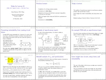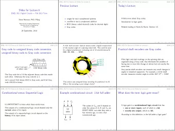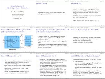
Slides for Lecture 7 ENCM 501: Principles of Computer Architecture - PowerPoint PPT Presentation
Slides for Lecture 7 ENCM 501: Principles of Computer Architecture Winter 2014 Term Steve Norman, PhD, PEng Electrical & Computer Engineering Schulich School of Engineering University of Calgary 30 January, 2014 slide 2/31 ENCM 501 W14
Slides for Lecture 7 ENCM 501: Principles of Computer Architecture Winter 2014 Term Steve Norman, PhD, PEng Electrical & Computer Engineering Schulich School of Engineering University of Calgary 30 January, 2014
slide 2/31 ENCM 501 W14 Slides for Lecture 7 Previous Lecture ◮ endianness ◮ addressing modes ◮ examples of tradeoffs in instruction set design
slide 3/31 ENCM 501 W14 Slides for Lecture 7 Today’s Lecture ◮ completion of previous lecture ◮ introduction to memory systems ◮ review of SRAM and DRAM Related reading in Hennessy & Patterson: Sections 2.1, B.1
slide 4/31 ENCM 501 W14 Slides for Lecture 7 Conditional branch options Most ISAs make branch decisions based on a few bits called flag bits or condition code bits that sit within some kind of processor status register . Let’s look at this for a simple C example, in which j and k are int variables in registers: if (i < k) goto L1; x86-64 translation, assuming i in %eax , k in %edx : cmpl %edx, %eax # compare registers jl L1 # branch based on N and V flags jl means “jump if less than.” (Note: In reality the assembly language label almost certainly won’t be the same as the C label L1 .)
slide 5/31 ENCM 501 W14 Slides for Lecture 7 For the same C code, here is an ARM translation, assuming i in r0 , k in r1 : CMP r0, r1 ; compare registers BLT L1 ; branch based on N and V flags MIPS is unusual—the comparison result goes into a GPR. Suppose we have i in R4 , k in R5 . . . SLT R8, R4, R5 # R8 = (R4 < R5) BNE R8, R0, L1 # branch if R8 != 0
slide 6/31 ENCM 501 W14 Slides for Lecture 7 Conditional instructions in ARM Recall from Assignment 1 that MIPS offers the conditional move instructions MOVN and MOVZ . (MIPS also has some similar floating-point conditional move instructions). ARM takes this idea to the extreme— every ARM instruction is conditional! Bits 31–28 of an ARM instruction are the so-called cond field, which specifies that the instruction either performs some action or is a no-op, depending on some condition on zero or more of the N, Z, V and C flags. Example ARM cond field patterns: ◮ 1110, for ALWAYS. The instruction is never a no-op. This is the default cond field in ARM assembly language. ◮ 0000, for EQUAL. Execute the instruction if and only if the Z flag is 1.
slide 7/31 ENCM 501 W14 Slides for Lecture 7 The power of ARM conditional instructions is illustrated by this example . . . Here is some C code: if (i == 33 || i == 63) count++; If i and count are int s in ARM registers r0 and r1 , here is ARM assembly language for the C code: TEQ r0, #33 ; # indicates immediate mode TEQNE r0, #63 ADDEQ r1, r1, #1 ; Note typo in Lec 6 slides! The cond field for the first instruction is 1110, for “always”. For the second instruction, it’s 0001, for “do it only if the Z flag is 0”, and for the third, it’s 0000, for “do it only if the Z flag is 1”.
slide 8/31 ENCM 501 W14 Slides for Lecture 7 Acknowledgment: Example on previous slide adapted from an example on pages 129–130 of Hohl, W., ARM Assembly Language: Fundamentals and Techniques , c � 2009, ARM (UK), published by CRC Press.
slide 9/31 ENCM 501 W14 Slides for Lecture 7 MIPS versus ARM: Vague arguments CPU time = IC × CPI × clock period MIPS attacks CPI by making instructions very simple and easy to pipeline. ARM tries to be close to MIPS with respect to CPI, and is much better than older CISC ISAs for CPI. ARM attacks IC by doing things in one instruction that might sometimes take two or three MIPS instructions.
slide 10/31 ENCM 501 W14 Slides for Lecture 7 MIPS versus ARM: How to be quantitative A fair and thorough study would require at least : ◮ real applications that are reasonably good fits for both ISAs; ◮ the best possible compilers for each of the ISAs; ◮ processors fabricated with the same transistor and interconnect technology, and very similar die sizes. Even then, it might not be a truly fair fight between ISAs, if one side has better digital designers than the other.
slide 11/31 ENCM 501 W14 Slides for Lecture 7 We’re moving on from ISA to microarchitecture For (much) more about ISA design considerations, see Appendix K of the textbook, which is available in PDF format as a no-charge download. The first aspect of microarchitecture we’ll look at is the memory hierarchy .
slide 12/31 ENCM 501 W14 Slides for Lecture 7 Views of memory: ISA versus microarchitecture (1) The modern ISA view of memory is simple: Memory is flat. For a program on a 32-bit system, a few regions within the address space from 0 to 0x ffff ffff are available. As long as alignment rules are respected, any memory read is pretty much the same as any other read, and any memory write is pretty much the same as any other write. The story is essentially the same for 64-bit systems, except that the maximum address is 0x ffff ffff ffff ffff . This simplicity is great for compiler writers choosing addressing modes for instructions, and for linker writers finding ways to stitch pieces of machine language together into complete machine language programs.
slide 13/31 ENCM 501 W14 Slides for Lecture 7 Views of memory: ISA versus microarchitecture (2) The modern microarchitecture view of memory is that memory is not at all simple! Modern memory systems are designed as complex hierarchies, with some subsystems optimized for high speed and others for large capacity and/or low cost. Energy use per memory access may be an important factor as well. Understanding of this kind of hierarchy is critical at several levels of computer engineering. Examples: ◮ selection of processors for embedded applications ◮ systems software development—operating system kernels, libraries, etc. ◮ application software development
slide 14/31 ENCM 501 W14 Slides for Lecture 7 Components within a memory system The schematic on the next page shows typical memory organization for a desktop computer in the time period from about 1999 to 2004. The box labeled CORE would contain GPRs, ALUs, control circuits and so on. TLB stands for translation lookaside buffer . A TLB does high-speed translation of virtual addresses into physical addresses . The core generates virtual addresses—PC values for instruction fetches, and data addresses generated by load and store instructions. Most cache designs are based on physical addresses, and the DRAM circuits definitely require physical addresses.
slide 15/31 ENCM 501 W14 Slides for Lecture 7 Sizes of boxes reflect neither chip area nor storage capacity! I-TLB DRAM CONTROLLER L1 I- CACHE UNIFIED DRAM CORE L2 MODULES CACHE D-TLB L1 D- CACHE The yellow box shows what would be included in a processor chip in the 1999–2004 time frame. In 2014, a quad-core chip would include four copies of everything in yellow, plus a large L3 cache shared by all four cores. The DRAM controller would be on-chip.
slide 16/31 ENCM 501 W14 Slides for Lecture 7 What are caches for? In trying to make sense of the complicated interconnections and interactions between caches it really helps to keep in mind what problems are solved by caches and what very different problems are solved by virtual memory. Let’s start with caches . Caches exist to optimize performance in the face of some difficult facts: ◮ DRAM latency is on the order of 100 processor clock cycles ◮ latency in small SRAM arrays is on the order of 1 processor clock cycle ◮ latency in larger SRAM arrays is on the order of 10 processor clock cycles
slide 17/31 ENCM 501 W14 Slides for Lecture 7 What is virtual memory for? Virtual memory is a system that operating system kernels can use to support applications. Some of the key benefits are: ◮ Protection. Each process —each running user program—has its own virtual address space. Processes cannot accidentally or maliciously access each other’s memory. ◮ Efficient memory allocation. A kernel can give an application a large contiguous piece of virtual address space made from many fragmented pieces of physical address space. ◮ Spilling to disk. If DRAM gets close to full, the kernel can copy pages of application memory to disk—the effective memory available can be greater than the DRAM capacity.
slide 18/31 ENCM 501 W14 Slides for Lecture 7 SRAM and DRAM Before looking in detail at how caches work, let’s look at the two main kinds of volatile storage in use in computer systems.
slide 19/31 ENCM 501 W14 Slides for Lecture 7 The “6T” SRAM (Static RAM) cell BITLINE BITLINE WORDLINE Q QN Q near V DD is a stored 1, and Q near ground is a stored 0. It’s called static RAM because in normal operation, and with WORDLINE low, the voltages at nodes Q and QN are stable. The bistable pair of inverters corrects for the effects of noise and leakage currents.
slide 20/31 ENCM 501 W14 Slides for Lecture 7 Writing a 1 to an SRAM cell BITLINE BITLINE WORDLINE Q QN Set BITLINE to V DD and BITLINE to 0. Turn on WORDLINE . If Q was previously 0, the signals on the bitlines overpower the inverter pair, making QN 0 and Q 1. If Q was already 1, nothing much happens in the cell. (To write a 0, Set BITLINE to 0 and BITLINE to V DD .)
Recommend
More recommend
Explore More Topics
Stay informed with curated content and fresh updates.
![MARKDOWN SLIDES [EN] MARKDOWN SLIDES [EN] MARKDOWN SLIDES [EN] MARKDOWN SLIDES [EN] MARKDOWN](https://c.sambuz.com/818511/markdown-slides-en-markdown-slides-en-markdown-slides-en-s.webp)


