Slides for Lecture 36 ENEL 353: Digital Circuits Fall 2013 Term - PowerPoint PPT Presentation
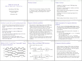
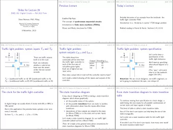
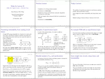
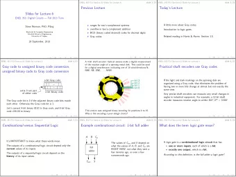
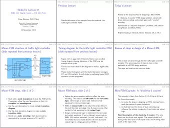
Slides for Lecture 36 ENEL 353: Digital Circuits Fall 2013 Term Steve Norman, PhD, PEng Electrical & Computer Engineering Schulich School of Engineering University of Calgary 4 December, 2013 slide 2/21 ENEL 353 F13 Section 02 Slides
Slides for Lecture 36 ENEL 353: Digital Circuits — Fall 2013 Term Steve Norman, PhD, PEng Electrical & Computer Engineering Schulich School of Engineering University of Calgary 4 December, 2013
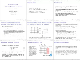
slide 2/21 ENEL 353 F13 Section 02 Slides for Lecture 36 Previous Lecture Completion of coverage of memory arrays, including use of ROM circuits to implement combinational logic functions.
slide 3/21 ENEL 353 F13 Section 02 Slides for Lecture 36 Today’s Lecture PLAs (programmable logic arrays). Related reading in Harris & Harris: Section 5.6.1
slide 4/21 ENEL 353 F13 Section 02 Slides for Lecture 36 What’s left in ENEL 353 in Fall 2013? Lecture Fri Dec 6. Comments about the final exam, and review of course content. Mon Dec 16: A Very Big Quiz.
slide 5/21 ENEL 353 F13 Section 02 Slides for Lecture 36 PLAs: Programmable logic arrays As explained in the previous lecture, any combinational circuit element can be implemented as a ROM circuit with the appropriate numbers of address inputs and data outputs. However, ROM implementation of combinational logic has some drawbacks: ◮ The size of the decoder grows exponentially with the number of input bits. ◮ Propagation delays may be lengthy due to relatively slow voltage changes on long bitlines. A PLA — programmable logic array —is a structure that allows SOP-based implementation of combinational logic in a way that may be more efficient than a ROM array.
slide 6/21 ENEL 353 F13 Section 02 Slides for Lecture 36 Review of terminology related to SOP expressions Literal: Either an input variable or its complement. If the input variables are A , B , C , then the available literals are A , ¯ A , B , ¯ B , C , ¯ C . Product: Either a literal, or two or more literals ANDed together. Minterm: A product that includes literals from all of the input variables. Implicant: A product is an implicant of Y if it can be included in a sum-of-products (SOP) expression for Y .
slide 7/21 ENEL 353 F13 Section 02 Slides for Lecture 36 What products are available? Let’s look at the example of a 3-input system with inputs A , B , C . All of the literals are products: A , ¯ A , B , ¯ B , C , ¯ C . All of the minterms are products: A ¯ ¯ B ¯ C , ¯ A ¯ BC , ¯ AB ¯ C , ¯ ABC , A ¯ B ¯ C , A ¯ BC , AB ¯ C , ABC . There are a lot of products that are neither literals nor minterms: A ¯ ¯ B , ¯ AB , A ¯ B , AB , ¯ A ¯ C , ¯ AC , A ¯ C , AC , ¯ B ¯ C , ¯ BC , B ¯ C , BC . As the number of input variables goes from 3 to 4 to 5 and beyond, the number of literals, minterms, and non-literal- non-minterm products gets very big, very fast. A key aspect of PLAs is the ability to select products with whatever number of literals makes sense .
slide 8/21 ENEL 353 F13 Section 02 Slides for Lecture 36 A generic M × N × P PLA inputs M AND implicants OR array array N P outputs The AND array generates all the products (implicants) that are needed in SOP expressions for the outputs. The OR array does the work of ORing together implicants to generate outputs.
slide 9/21 ENEL 353 F13 Section 02 Slides for Lecture 36 Dot notation for PLAs (and ROM arrays) In diagrams for PLAs and ROMs, a dot on a pair of crossing wires never indicates simple electrical connection of the two wires! Review: What does a dot indicate in a ROM diagram? Let’s write down what dots mean in PLA diagrams.
slide 10/21 ENEL 353 F13 Section 02 Slides for Lecture 36 An example PLA, shown with dot notation Note the use of inverters to generate complements of the input variables. A B C OR array n3 n2 n1 n0 AND array Y 1 Y 0 What are the dimensions M, N, and P? Give algebraic expressions for Y 1 and Y 0 .
slide 11/21 ENEL 353 F13 Section 02 Slides for Lecture 36 PLA design example #1 A B C Y 1 Y 0 0 0 0 0 0 Let’s implement the given truth 0 0 1 1 1 table using a 3 × 3 × 2 PLA. 0 1 0 0 0 The solution is not unique. 0 1 1 1 1 What are two different SOP 1 0 0 0 1 expressions that work for Y 1 ? 1 0 1 1 0 1 1 0 0 0 1 1 1 0 0
slide 12/21 ENEL 353 F13 Section 02 Slides for Lecture 36 How many implicant wires should a PLA have? Typically N , the number of implicant wires, is significantly less than 2 M , where M is the number of inputs. Why would it make no sense at all to have N > 2 M ?
slide 13/21 ENEL 353 F13 Section 02 Slides for Lecture 36 PLA design example #2 Suppose you have these K-maps and have been asked to implement the logic using a 3 × 3 × 2 PLA. Y 1 Y 0 A B A B 00 01 11 10 00 01 11 10 C C 0 0 1 1 1 1 1 1 1 1 What goes wrong if you use the K-maps to find separate minimal SOP expressions for Y 1 and Y 0 ? By looking at the K-maps again, let’s find SOP expressions that will work for the PLA.
slide 14/21 ENEL 353 F13 Section 02 Slides for Lecture 36 PLA implementation with NMOS transistors Y 1 = AB + ¯ BC and Y 0 = AB in this 3 × 2 × 2 PLA. You can tell from the dots! But why does this circuit work? A B C OR array R R n1 R n0 R AND array Y 1 Y 0
slide 15/21 ENEL 353 F13 Section 02 Slides for Lecture 36 How does the AND array work? For example, why is it that n1 = AB? A B C OR array R R n1 R n0 R AND array Y 1 Y 0
slide 16/21 ENEL 353 F13 Section 02 Slides for Lecture 36 How does the OR array work? For example, why is it that Y 1 = n1 + n0 ? A B C OR array R R n1 R n0 R n3 n2 AND array Y 1 Y 0
slide 17/21 ENEL 353 F13 Section 02 Slides for Lecture 36 The textbook on ROM and PLA implementations with NMOS transistors Section 5.6.3 in Harris & Harris covers this topic. Unfortunately, Figure 5.63 has a couple of confusing typographical errors, which are not hard to spot if you compare it to Figure 5.55 . . . ◮ There is a missing dot in the AND array. ◮ The implicant labeled as AB should be labeled A ¯ B .
slide 18/21 ENEL 353 F13 Section 02 Slides for Lecture 36 PLA implemented with floating-gate transistors A B C OR array R R R R AND array Y 1 Y 0 Put neutral charge on floating gates wherever an NMOS transistor is needed. Put negative charge on floating gates wherever the absence of an NMOS transistor is needed.
slide 19/21 ENEL 353 F13 Section 02 Slides for Lecture 36 Why study PLAs in a course like ENEL 353? The idea that a chip that is just a single PLA could be commercially viable has been obsolete for decades. (Tens of years, not tens of clock cycles!) A typical programmable logic chip in 2013 is much more powerful and much faster than a PLA. So why study PLAs? ◮ PLA design provides an excellent review of some fundamental concepts in combinational logic design. ◮ Use of PLA-like structures within a larger digital integrated circuit design still makes sense. ◮ Instructors like to make up exam questions about PLAs.
slide 20/21 ENEL 353 F13 Section 02 Slides for Lecture 36 Examinable material ended a few slides back Let’s make a note of exactly where the examinable material ended!
slide 21/21 ENEL 353 F13 Section 02 Slides for Lecture 36 Best of luck on the ENEL 353 final and all your other exams! Happy Holidays!
Recommend
More recommend
Explore More Topics
Stay informed with curated content and fresh updates.
![MARKDOWN SLIDES [EN] MARKDOWN SLIDES [EN] MARKDOWN SLIDES [EN] MARKDOWN SLIDES [EN] MARKDOWN](https://c.sambuz.com/818511/markdown-slides-en-markdown-slides-en-markdown-slides-en-s.webp)

