Slides for Lecture 29 ENEL 353: Digital Circuits Fall 2013 Term - PowerPoint PPT Presentation
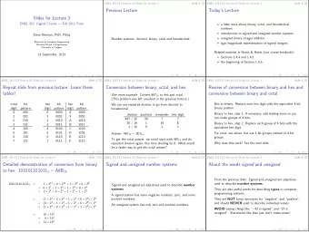
Slides for Lecture 29 ENEL 353: Digital Circuits Fall 2013 Term Steve Norman, PhD, PEng Electrical & Computer Engineering Schulich School of Engineering University of Calgary 18 November, 2013 slide 2/17 ENEL 353 F13 Section 02
Slides for Lecture 29 ENEL 353: Digital Circuits — Fall 2013 Term Steve Norman, PhD, PEng Electrical & Computer Engineering Schulich School of Engineering University of Calgary 18 November, 2013
slide 2/17 ENEL 353 F13 Section 02 Slides for Lecture 29 Previous Lecture Completion of “divide-by-3 counter” FSM design using one-hot state encoding. Introduction to “sequence detection” problems, and solution using Moore and Mealy FSMs. Moore and Mealy state transition diagrams for an example sequence detection problem.
slide 3/17 ENEL 353 F13 Section 02 Slides for Lecture 29 Today’s Lecture Completion of next-state and output logic design for the Mealy FSM solution to example sequence detection problem. Factoring of FSMs. Reverse-engineering an FSM: Given an FSM circuit, find a word description of what the FSM does. Introduction to timing of sequential logic. Related reading in Harris & Harris: Sections 3.4.3–3.4.6, introduction to Section 3.5.
slide 4/17 ENEL 353 F13 Section 02 Slides for Lecture 29 Review: State transition diagram for Mealy FSM solution to example sequence detection problem In diagrams for Mealy FSMs, it doesn’t make 0/0 sense to put output values 1/0 in the state circles. reset S0 S1 Arcs are labeled in / out . 0/0 in indicates the input 0/1 1/0 value that causes a state 0/0 transition. out indicates S3 S2 the output value for the 1/0 given input and the state 1/0 that the arc is coming from .
slide 5/17 ENEL 353 F13 Section 02 Slides for Lecture 29 Sequence detection example: Mealy FSM, continued Let’s choose unsigned binary encoding of the states. Let’s make a combined state transition and output table. (We’ll go straight to the version that is based on our chosen state encoding, because for this example, that’s pretty easy to do without a version of the table that lists the states symbolically.) Let’s find next-state and output equations. Let’s draw a schematic.
slide 6/17 ENEL 353 F13 Section 02 Slides for Lecture 29 Sequence detection FSMs with an “unreasonable” input signal Let’s determine what the Moore and Mealy FSMs will do if the input A is as shown . . . 1 CLK 0 1 reset 0 1 A 0 1 Y (Moore) 0 1 Y (Mealy) 0 t 0 t 1 t 2 t 3 t 4 Let’s make a few remarks.
slide 7/17 ENEL 353 F13 Section 02 Slides for Lecture 29 A revised traffic light problem B. Blvd N In regular mode , the system behaves like the W E system that’s already S been designed. In parade mode , the A. Ave system advances through the regular sequence until it gets to red for A and green for B, then stays in that state . Let’s make a block diagram showing the inputs and outputs of the new, more complex traffic light controller.
slide 8/17 ENEL 353 F13 Section 02 Slides for Lecture 29 Revised traffic light problem: Most obvious FSM solution One approach to the problem is to make a new design with eight states: ◮ four states for regular mode; ◮ four more states for parade mode. Why are four different states needed for parade mode? The eight-state FSM idea leads to the messy state transition diagram on the next slide . . .
8-state transition diagram for traffic light system with “parade mode” P T A P T A R T A R T A Reset P T A S0 S1 R T A R T A S4 S5 L A : green L A : yellow P L B : red L B : red L A : green L A : yellow L B : red L B : red R P P T A P R P R P T B R S3 S2 S7 S6 L A : red L A : red L B : yellow L B : green L A : red L A : red P T B L B : yellow L B : green R P R T B R T B Image is taken from Figure 3.34 from Harris D. M. and Harris S. L., Digital Design and Computer Architecture, 2nd ed. , c � 2013, Elsevier, Inc.
slide 10/17 ENEL 353 F13 Section 02 Slides for Lecture 29 Factoring FSMs The parade-mode example is set up to make two main points: ◮ Trying to solve every synchronous sequential system design problem with a single FSM may result in unreasonably complex FSM designs. ◮ FSMs are nevertheless a great design tool. Sometimes it make sense to design a system as a collection of simple, collaborating FSMs. Factoring is the name given to the approach described in the second of the above two points. Let’s draw a block diagram to show how the traffic light controller with parade mode can be designed using two simple FSMs that work together.
slide 11/17 ENEL 353 F13 Section 02 Slides for Lecture 29 State transition diagrams for factored FSM design T A Reset T A S0 S1 L A : green L A : yellow L B : red L B : red P Reset P S3 S2 S0 S1 L A : red L A : red M: 0 M: 1 L B : yellow L B : green R MT B M + T B R Lights FSM Mode FSM Image is taken from Figure 3.34 from Harris D. M. and Harris S. L., Digital Design and Computer Architecture, 2nd ed. , c � 2013, Elsevier, Inc.
slide 12/17 ENEL 353 F13 Section 02 Slides for Lecture 29 Deriving an FSM from a schematic The next few slides closely follow the process used in Section 3.4.5 of the textbook, but use a completely different example schematic. (It’s a good idea to study the textbook example as well as the lecture example.) The first two steps in “reverse engineering” the schematic of an FSM are: ◮ Examine circuit, stating inputs, outputs, and state bits. ◮ Write next-state and output equations. Let’s perform those two steps for the schematic on the next slide . . .
slide 13/17 S 2 S 1 S 0 CLK S ′ S 2 2 Y 2 S ′ S 1 1 Y 1 S ′ S 0 0 Y 0 r reset A
slide 14/17 S 2 S 1 S 0 A S ′ 2 S ′ 1 S ′ The next three steps are: 0 0 0 0 0 0 0 0 ◮ Use next-state and output 0 0 0 1 0 0 1 equations to create 0 0 1 0 0 0 1 next-state and output 0 0 1 1 0 1 0 tables. (The next-state 0 1 0 0 0 1 0 table is ready for us on this 0 1 0 1 0 1 1 slide, to save us all some 0 1 1 0 0 1 1 boredom.) 0 1 1 1 1 0 0 ◮ Reduce the next-state table 1 0 0 0 1 0 0 1 0 0 1 0 0 0 to eliminate unreachable 1 0 1 0 0 0 0 states. 1 0 1 1 0 0 0 ◮ Assign each valid state bit 1 1 0 0 0 0 0 combination a name. 1 1 0 1 0 0 0 Let’s perform the last two of the 1 1 1 0 0 0 0 above steps. 1 1 1 1 0 0 0
slide 15/17 ENEL 353 F13 Section 02 Slides for Lecture 29 Completion of the example FSM derivation problem The final three steps are: ◮ Rewrite next-state and output tables with state names. ◮ Draw state transition diagram. ◮ State in words what the FSM does. Let’s work through these steps.
slide 16/17 ENEL 353 F13 Section 02 Slides for Lecture 29 Introduction to timing of sequential logic For a synchronous sequential circuit design, some of the major timing concerns are . . . ◮ What are sufficient conditions on the D input of a DFF to ensure reliable operations of the DFF? (This is called the “dynamic discipline”.) ◮ Given timing specifications for DFFs and a desired clock period T C , what do those things say about maximum delays in combinational elements in the circuit? ◮ What can go wrong if D inputs of DFFs go 0 → 1 or 1 → 0 at the wrong time? Section 3.5 of Harris & Harris is excellent on these topics. Please read it carefully, more than once!
slide 17/17 ENEL 353 F13 Section 02 Slides for Lecture 29 Upcoming topics Timing of sequential logic. Related reading in Harris & Harris: Section 3.5 up to the end of 3.5.2.
Recommend
More recommend
Explore More Topics
Stay informed with curated content and fresh updates.
![MARKDOWN SLIDES [EN] MARKDOWN SLIDES [EN] MARKDOWN SLIDES [EN] MARKDOWN SLIDES [EN] MARKDOWN](https://c.sambuz.com/818511/markdown-slides-en-markdown-slides-en-markdown-slides-en-s.webp)


