Slides for Lecture 18 ENEL 353: Digital Circuits Fall 2013 Term - PowerPoint PPT Presentation
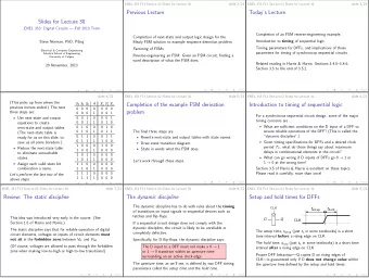
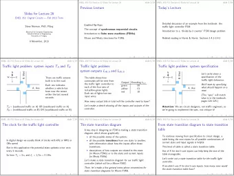
Slides for Lecture 18 ENEL 353: Digital Circuits Fall 2013 Term Steve Norman, PhD, PEng Electrical & Computer Engineering Schulich School of Engineering University of Calgary 21 October, 2013 slide 2/22 ENEL 353 F13 Section 02 Slides
Slides for Lecture 18 ENEL 353: Digital Circuits — Fall 2013 Term Steve Norman, PhD, PEng Electrical & Computer Engineering Schulich School of Engineering University of Calgary 21 October, 2013
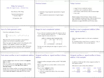
slide 2/22 ENEL 353 F13 Section 02 Slides for Lecture 18 Previous Lecture Completion of material on don’t-care outputs and inputs. Using K-maps to find minimal POS (not SOP) expressions. If time permitted . . . K-maps for problems with 5 inputs.
slide 3/22 ENEL 353 F13 Section 02 Slides for Lecture 18 Today’s Lecture Completion of material on K-maps with 5 or 6 input bits. (Related reading in Harris & Harris: None.) Using K-maps for problems with multiple output bits. (Related reading in Harris & Harris: None.) Multiplexers. (Related reading in Harris & Harris: Section 2.8 introduction and Section 2.8.1.)
slide 4/22 ENEL 353 F13 Section 02 Slides for Lecture 18 K-maps with more than four variables With three or four variables, adjacent cells are easy to spot, as long as you remember to look for groups that wrap around the edges of a map. With five or six variables, it’s more difficult to organize cells to make all adjacencies easy to discover. There are a few different options for setting up 5- and 6-variable maps. We’ll follow the method outlined in last year’s ENEL 353 textbook. (Marcovitz A. B., Introduction to Logic Design, 3rd ed. , 2010, McGraw-Hill.)
slide 5/22 ENEL 353 F13 Section 02 Slides for Lecture 18 A 3-dimensional map for a 5-variable problem We can visualize the 32-cell map this way: We look for vertical adjacencies as well as the horizontal adjacencies we’re used to finding in 4-variable maps. But marking and grouping 1-cells in a sketch like that is pretty much impossible . . .
slide 6/22 ENEL 353 F13 Section 02 Slides for Lecture 18 2-dimensional representation of the 3-d map F ( A , B , C , D , E ) B C 00 01 11 10 D E 00 01 B C 00 01 11 10 D E 11 00 10 01 11 top layer: A = 0 10 bottom layer: A = 1 The five yellow cells are all adjacent to the blue cell.
slide 7/22 ENEL 353 F13 Section 02 Slides for Lecture 18 Example 5-variable problem Find a minimal SOP expression for F ( A , B , C , D , E ) = Σ(3 , 6 , 11 , 14 , 22 , 24 , 28 , 30)
slide 8/22 ENEL 353 F13 Section 02 Slides for Lecture 18 Example 5-variable problem: Solution B B B C B C 00 01 11 10 00 01 11 10 D E D E 0 4 12 8 16 20 28 24 00 00 1 1 1 5 13 9 17 21 29 25 01 01 E E 3 7 15 11 19 23 31 27 11 11 1 1 D D 2 6 14 10 18 22 30 26 10 10 1 1 1 1 C C A = 0 A = 1 F ( A , B , C , D , E ) = ¯ A ¯ CDE + AB ¯ D ¯ E + CD ¯ E
slide 9/22 ENEL 353 F13 Section 02 Slides for Lecture 18 6-variable K-maps Visualize a 4 × 4 × 4 cube of 64 cells. Gray code ordering must be used in the vertical direction as well as the two horizontal directions. This year in ENEL 353 we will not do detailed examples of 6-variable K-maps, and you will not be tested on 6-variable K-maps.
slide 10/22 ENEL 353 F13 Section 02 Slides for Lecture 18 Multiple-output minimization problems It’s common to have combinational logic systems that have multiple outputs depending on the same inputs . It makes sense to look for ways to share logic gates between two or more functions . . . Separate circuits for F , G , H Opportunity to share circuitry in producing F , G , H A B F A C F B D G C H D G H
An example 3-output problem: Here are K-maps for function F , G , and H , with common inputs A , B , C , and D . . . F ( A , B , C , D ) G ( A , B , C , D ) H ( A , B , C , D ) A B A B A B 00 01 11 10 00 01 11 10 00 01 11 10 C D C D C D 00 00 1 1 00 01 1 1 01 1 1 01 1 11 1 1 11 11 1 1 1 10 1 1 10 10 The groupings of 1-cells above show minimal SOP expressions for each of the outputs considered independently of the other two . . . F = ¯ AD + AC ¯ D 2 AND gates, 1 OR gate G = ¯ A ¯ CD + B ¯ C ¯ 2 AND gates, 1 OR gate D H = ¯ ACD + A ¯ BD 2 AND gates, 1 OR gate
By splitting one of the prime implicants of F we can share products that are already in use for G and H . . . F ( A , B , C , D ) G ( A , B , C , D ) H ( A , B , C , D ) A B A B A B 00 01 11 10 00 01 11 10 00 01 11 10 C D C D C D 00 00 1 1 00 01 1 1 01 1 1 01 1 11 1 1 11 11 1 1 1 10 1 1 10 10 The number of OR gates is 3, same as before, but the number of AND gates has been reduced to 5 from 6 . . . F = ¯ A ¯ CD + ¯ ACD + AC ¯ D G = ¯ A ¯ CD + B ¯ C ¯ D H = ¯ ACD + A ¯ BD However, the OR gate that produces F now needs 3 inputs instead of 2.
slide 13/22 ENEL 353 F13 Section 02 Slides for Lecture 18 Multiple-output problems: Remarks The example shows that building minimal SOP expressions from prime implicants of individual outputs does not always minimize the overall number of products required to generate all the outputs with two-level SOP logic. Finding minimum-cost circuits for multiple output circuits has been a topic in past versions of ENEL 353, but in Fall 2013, we will not explore this topic in detail.
slide 14/22 ENEL 353 F13 Section 02 Slides for Lecture 18 Combinational building blocks Recent lectures and reading about algebra and K-maps have been oriented towards gate-level circuit designs to implement given logic functions. However, circuit designers can often be more productive by thinking in terms of combinational building blocks , combinational elements that are more complex than simple AND, OR, NAND, NOR and XOR gates. We’ve already studied one such building block: the one-bit full adder . We’re now going to look at two more important kinds of bulding block: multiplexers and decoders .
slide 15/22 ENEL 353 F13 Section 02 Slides for Lecture 18 Multiplexers Multiplexer is rather a long word, so mux is often used as an abbreviation. Another quite descriptive name for multiplexer is selector . A multiplexer circuit has ◮ two or more data inputs ; ◮ one or more bits of select input ; ◮ an output. The job of a multiplexer is to copy one of the data inputs to the output . The data input selected for copying is chosen by the select input.
slide 16/22 ENEL 353 F13 Section 02 Slides for Lecture 18 The 2:1 multiplexer (“two-to-one mux”) A circuit symbol and truth table: D 1 D 0 S Y 0 0 0 0 S 0 0 1 0 0 1 0 1 D 0 0 0 1 1 0 Y 1 0 0 0 D 1 1 1 0 1 1 1 1 0 1 1 1 1 1 Let’s write out a few sentences to describe exactly what this circuit does.
slide 17/22 ENEL 353 F13 Section 02 Slides for Lecture 18 2:1 mux — built from NOT, AND and OR gates The truth table from the previous slide results in this K-map and minimal SOP expression . . . D 1 D 0 00 01 11 10 S Y = D 0 ¯ S + D 1 S 0 1 1 1 1 1 S A circuit for this made from NOT, AND, and OR D 0 gates . . . Y D 1
slide 18/22 ENEL 353 F13 Section 02 Slides for Lecture 18 Variations on the tristate buffer (a) (b) E E A Y A Y non-inverting, non-inverting, active high enable active low enable (c) E (d) E A Y A Y inverting, inverting, active high enable active low enable Version (a) is the one we have already looked at. But each of (b), (c), and (d) is sometimes useful as well. Let’s make tables to describe all four circuits.
slide 19/22 ENEL 353 F13 Section 02 Slides for Lecture 18 2:1 mux implemented with tristate buffers The two schematics describe exactly the same design . The one on the right is from the textbook, and uses a compact notation for showing a common control input wire for the tristate buffers. S S D 0 T0 D 0 T0 Y Y D 1 D 1 T1 T1 Two gate outputs are wired together! Is that a problem in this design? Image on right is from Figure 2.56 from Harris D. M. and Harris S. L., Digital Design and Computer Architecture, 2nd ed. , c � 2013, Elsevier, Inc.
slide 20/22 ENEL 353 F13 Section 02 Slides for Lecture 18 The 4:1 multiplexer (“four-to-one mux”) S 1 S 0 How many rows would a truth table D 0 00 for this circuit have? D 1 01 Let’s describe the circuit in a table Y that is more compact than a truth D 2 10 table. D 3 11
Let’s make some notes on these three designs for 4:1 mux circuits. S 1 S 0 S 1 S 0 D 0 D 0 S 1 S 0 D 1 S 0 S 1 D 1 D 2 D 0 0 S 1 S 0 Y D 1 1 D 3 0 D 2 Y 1 S 1 S 0 D 2 0 D 3 D 3 1 Y (a) (b) (c) Image is Figure 2.58 from Harris D. M. and Harris S. L., Digital Design and Computer Architecture, 2nd ed. , c � 2013, Elsevier, Inc.
slide 22/22 ENEL 353 F13 Section 02 Slides for Lecture 18 Upcoming topics Using multiplexers to implement combinational logic functions. Decoders. Related reading in Harris & Harris: Sections 2.8.1 and 2.8.2.
Recommend
More recommend
Explore More Topics
Stay informed with curated content and fresh updates.
![MARKDOWN SLIDES [EN] MARKDOWN SLIDES [EN] MARKDOWN SLIDES [EN] MARKDOWN SLIDES [EN] MARKDOWN](https://c.sambuz.com/818511/markdown-slides-en-markdown-slides-en-markdown-slides-en-s.webp)

