Series 7 Clocking Clocks need to be treated differently than other - PowerPoint PPT Presentation
Series 7 Clocking Clocks need to be treated differently than other signals within the device. Globally accessible Minimal offset across the entire device Handle high fan out Dedicated Resources to generating and routing clock
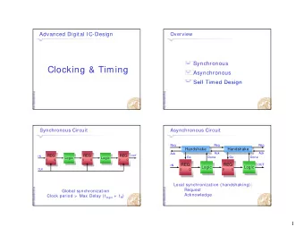
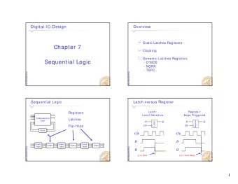
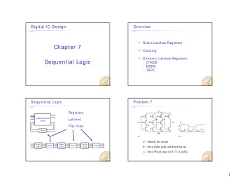
Series 7 Clocking • Clocks need to be treated differently than other signals within the device. • Globally accessible • Minimal offset across the entire device • Handle high fan out • Dedicated Resources to generating and routing clock signals. • Xilinx UG 472 • Incorrect understanding and use of clocks is one of the main causes in loss of coherency/stability in digital systems. • SNR is significantly reduced when coherency is lost.
Clock, Trigger, & Data Routing DAC CLK (64 GHz) DIV-BY-256 REF CLK CLK_IN & SYNC DIV-BY-2 (250 MHz) (125 MHz) TRIGGER IN LATCH LATCH PFI2 (250 MHz) EPRI (125 MHz) CLK CLK MARKER 1 LATCH LATCH PFI0 PRIs at a PRI ADJ factor of (125 MHz) DELAY 125 MHz CLK CLK MARKER 2 LATCH LATCH PFI4 WAVE ID DATA 125/N MHz (125 MHz) BAUD CLK CLK DACs OUT LATCH LATCH AIN 0- π CHIRP 2-Samples N/125 MHz at 125 MHz DURATION CLK CLK (250 MHz)
High Level Clock Architecture • 1 to 24 Clock Regions (Horizontal) • A Clock Region Contains • 50x CLBs per column • 10x 36k Block RAMs • 20x DSP Slices • 12x BUFHs to Route clocks across the horizontal clock region • MMCM and PLL • Mixed-Mode Clock Manager • Phase Locked Loop • BUFG are used to route clocks throughout the entire device.
Buffers • BUFG – Global Clock Buffer • Accessible anywhere in the device. • 1 input and 1 output. • BUFGCE(_1) • Same as BUFG with CE input. • _1: output is one when CE=0. • BUFGCTRL – Global Clk Buf Control • MUXES two clock inputs. • Includes CE’s. • BUFGMUX(_1) • Simple version of BUFGCTRL • BUFMUX_CTRL – same ...
Buffers • BUFH, BUFHCE(_1) • HROW. • Limited to a single clocking region. • BUFIO • Routes clock for IO Resources. • BUFMR, BUFMRCE • Multiple Region. • BUFR • Regional. • Includes ATTRIBUTES for Divider (1-8).
Clock Management Tile • Very Similar • Capability to generate various frequencies and phase offsets between multiple clocks. • Why do we need different clocks. • Decimation • Different timing requirements • DDR, ... • Gigabit Transcievers. • IO serializers and deserializers
MMCM and PLL • Very Similar • Capability to generate various frequencies and phase offsets between multiple clocks. • Why do we need different clocks. • Decimation • Different timing requirements • DDR, ... • Gigabit Transcievers. • IO serializers and deserializers
MMCM and PLL • See clk_mgmt.v
Routing MMCM/PLLs • Basic feedback. • No need for phase alignment on input and outputs.
Routing MMCM/PLLs • Using BUFG(or H) feedback. • Phase Aligned
Routing MMCM/PLLs • Using BUFG(or H) feedback. • Phase Aligned
Clocks for I/O Resources • serializers
Digital Signal Processing ● Most DSP application involve delays, multiplication, accumulation. – Filters – FFT s – I & Q Modulation
DSP48E1 Primitive The Series 7 devices includes a number of DSP48E1 Blocks on the device. • 25-bit pre-adder/subtractor • 25x18-bit multiplier • 48-bit post-adder/subtractor • Delay registers with optional bypasses (set in the configuration bit file)
Inputs ● 4 main data inputs D: 25-bit input to pre-adder/subtractor. – A: 25-bit input to pre-adder/subtractor or direct input to the – multiplier. B: 18-bit input to the multiplier. – C: 48-bit input to the post-adder/subtractor. – ● Other inputs – BCIN: 18-bit carry input to 18-bit pre-adder. PCIN: – 48-bit carry input to 48-bit post-adder. – CIN: 1-bit carry input to 48-bit post-adder. – opmode: 7-bit control for add/subtract and routing.
Outputs – P: main output from 48-bit post-adder. – PCOUT: Same only carry output. – BCOUT: Carry output from 18-bit pre-adder. – MFOUT: 48-bit output from the multiplier. – CCOUT (CFOUT): 1-bit carry output from 48-bit post- adder.
Block Diagram
Block Diagram
FIR Filter Design ● Basic building block of a tapped delay line FIR filter is a delay, multiply, and add sequence. – delay input and output – multiplier with tap weight – accumulator input and output
Block Diagram
Mixer DDS X FIR
SSB DDS X + X DDS
Recommend
More recommend
Explore More Topics
Stay informed with curated content and fresh updates.
