IN3170/4170, Spring 2020 Philipp Hfliger hafliger@ifi.uio.no - PowerPoint PPT Presentation
IN3170/4170, Spring 2020 Philipp Hfliger hafliger@ifi.uio.no Excerpt of formar INF2270 script Chapter 6: Sequential Logic Circuits Content Combinational Logic Single Bit Storage Sequential Logic Content Combinational Logic Single Bit
IN3170/4170, Spring 2020 Philipp Häfliger hafliger@ifi.uio.no Excerpt of formar INF2270 script Chapter 6: Sequential Logic Circuits
Content Combinational Logic Single Bit Storage Sequential Logic
Content Combinational Logic Single Bit Storage Sequential Logic
On Circuit Notation in INF2270 Script 2 bit Multiplexer ‘spelled out’ S S 1 0 a 0 c 0 2 b 0 a 2 AND2 simplifed to c b a 1 2 c 1 b 1 2 4 S decoder I 0 4 AND4 O 4 I I 1 simlifed to O 2 I 2 I 3
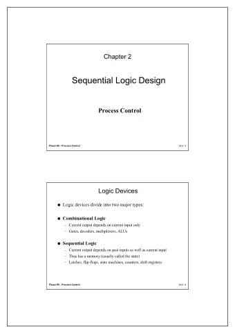
Combinational Logic Combinational logic circuits are feed-forward logic/digital circuits with no memory that can be described by Boolean functions. Note what is implied here: logic gates can also be connected in ways that include feed-back connections that implement/include memory that cannot be described as Boolean functions! This is then not ’combinational logic’, but ’sequential logic’, of which we will talk later.
Design and Analysis of Digital Circuits Design of a digital circuit is the process of assembling circuit blocks to form a bigger digital circuit. Analysis of a digital circuit is the process of finding out what it is doing, e.g. (in the case of combinational logic!) by finding an equivalent Boolean function or a complete truth table.
A complete analysis of a digital circuit is quite trivial for small digital circuits but neigh impossible for circuits of the complexity of a modern CPU. Hierarchical approaches in design and analysis provide some help. The first Pentium on the market had a mistake in its floating point unit. After the Intel 286 there was the 386 and then the 486, but the 585.764529 was then dubbed ’Pentium’ for simplicity sake.
Logic Gate Signals A certain range of input voltage is defined as ’high’ or logic ’1’ and another range is defined as ’low’ or ’0’. Note: the range is defined bigger at a logic gate input E.g. in a digital circuit with a 1.8V supply one can, for instance, guarantee an input voltage of 0V to 0.5V to be recognised as ’0’ and 1.2V to 1.8V as ’1’ by a logic gate. On the output side the gate can guarantee to deliver a voltage of either > 1.75V or < 0.05V. The assymetric ranges correct ‘errors’ in a cascade of gates, adding a safety margin between input and output, makeing (correctly designed!) digital circuits very robust (which is necessary with millions of logic gates in a CPU, where a single error might impair the global function!)
Analysis Example ≡ a ∧ ¯ a ∧ ¯ b ∨ b ∧ c ∨ ¯ b ∧ c ���� ���� � �� � x 4 x 5 x 6
Design Example (Universality of NAND and NOR) Design equivalent circuits with only NANDs (NORs) → → →
Design Example (Universality of NAND and NOR) Design equivalent circuits with only NANDs (NORs) → → →
Design Example (Universality of NAND and NOR) Design equivalent circuits with only NANDs (NORs) → → →
Design Example (Universality of NAND and NOR) Design equivalent circuits with only NANDs (NORs) → → →
Design Example (Universality of NAND and NOR) Design equivalent circuits with only NANDs (NORs) → → →
Design Example (Universality of NAND and NOR) Design equivalent circuits with only NANDs (NORs) → → →
Design Example (Universality of NAND and NOR) Design equivalent circuits with only NANDs (NORs) → → →
Standard Combinational Logic Some combinational logic (and of course also sequential logic → later) is often used in computational devices and are usually provided as ’black boxes’ guaranteeing a defined function. Examples: ◮ encoder/decoder ◮ multiplexer/demultiplexer ◮ adders/multipliers There are actually variations on how those functions are implemented, resulting in different processing speeds and/or power consumption and/or scalability (i.e. how easy it is to adapt the same function for more inputs).
3-bit Encoder Specification An encoder in digital electronics refers to a circuit that converts 2 n inputs (one-hot code) into n outputs (binary number), as specified by the following truth table.
Simple 3-bit Encoder Truth Table I 7 I 6 I 5 I 4 I 3 I 2 I 1 I 0 O 2 O 1 O 0 0 0 0 0 0 0 0 1 0 0 0 0 0 0 0 0 0 1 0 0 0 1 0 0 0 0 0 1 0 0 0 1 0 0 0 0 0 1 0 0 0 0 1 1 0 0 0 1 0 0 0 0 1 0 0 0 0 1 0 0 0 0 0 1 0 1 0 1 0 0 0 0 0 0 1 1 0 1 0 0 0 0 0 0 0 1 1 1
3-bit Encoder Implementation Variant
3-bit Encoder Remarks The truth table that was given is not complete: some inputs are ‘illegal’ (not one-hot codes). Circuitry that produces the input should ensure to only produce legal states. In our specific digital circuit implementation we can deduct what the output in each illegal case would be, but other implementation may provide different outputs in those non-defined cases, and still be valid encoders! The following truth table is a deterministic specification of an encoder, without ‘illegal’ inputs, where the ’highest’ active input bit determines the output. ’X’ in the table means ‘do not care’, or ‘for any state’ and allows to abbreviate the truth table. This would require a different implementation, but we will not present it here.
3-bit Priority Encoder Truth Table I 7 I 6 I 5 I 4 I 3 I 2 I 1 I 0 O 2 O 1 O 0 0 0 0 0 0 0 0 1 0 0 0 0 0 0 0 0 0 1 X 0 0 1 0 0 0 0 0 1 X X 0 1 0 0 0 0 0 1 X X X 0 1 1 0 0 0 1 X X X X 1 0 0 0 0 1 X X X X X 1 0 1 0 1 X X X X X X 1 1 0 1 X X X X X X X 1 1 1
Content Combinational Logic Single Bit Storage Sequential Logic
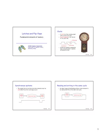
Flip-Flop Flip-flops are digital circuits with two stable states that are used as storage elements for 1 bit. The term ’flip-flop’ is in the more recent use of the language more specifically used for synchronous binary memory cells (e.g. D-flip-flop, JK-flip-flop, T-flip-flop), whereas the term ’latch’ (e.g. SR-latch, D-latch) is used for the simpler more basic asynchronous ’transparent’ storage elements, but this is not necessarily consequently applied throughout the literature.
Characteristic Table and Equation The behaviour of a flip-flop can be expressed with a characteristic table : a truth table expressing the relation between the input and the present state, and the next state. An alternative is the characteristic equation which defines the dependency of the next state on the input and present state as a Boolean expression. Examples follow on the next slides.
Flip-Flop Principle: Positive Feedback The simplest Flip Flop: Gated D-Latch/Transparent Latch Characteristic Equation: Q = D ∧ E ∨ ¯ E ∧ Q When the feedback loop is connected the state is maintained
D-Flip-Flop from D-Latch
Clock Signal
D-Flip-Flop Abbreviated: D Q t Q t + 1 Characteristic Table 0 X 0 D Q t Q t + 1 1 X 1 0 0 0 0 1 0 or simply: 1 0 1 D Q t + 1 1 1 1 0 0 Characteristic Equation: 1 1 Q = D
Content Combinational Logic Single Bit Storage Sequential Logic
Finite State Machines Finite State Machines (FSM) are a formal model suited to describe sequential logic, i.e. logic circuits who’s output does not only depend on the present input but on internal memory and thus, on the history or sequence of the inputs.
Specifying a FSM with a state transition graph Example: Traffic Light
Moore and Mealy Machine In a Moore FSM, the output depends solely on the state/memory, in contrast to the Mealy model , where outputs also depend on the inputs directly. The later sometimes allows to reduce the number of states, but is more demanding to design.
Synchronous and Asynchronous FSM ◮ Synchronous FSMs: transition of a global clock signal as implicit transition condition for all state changes. Realized as sequential logic circuits with synchronous flip-flops, e.g. D-flip-flops. Generally simpler to implement and easier to verify and test. The clock frequency needs to be slow enough to allow the slowest combinational transition condition to be computed. ◮ Asynchronous FSMs change state at once if the explicit transition condition is met (buzzword: ’ripple’). They can be very fast but are much harder to design and verify.
Deducing a Synchronous 3-bit Counter from a FSM Counters are a frequently used building block in digital electronics. A counter increases a binary number with each clock edge. For the design of this simple counter variant, state transitions are unconditional, i.e. they happen in every case at every positive clock edge.
State Transition Table present in next We chose to represent the 8 S 2 S 1 S 0 NA S 2 S 1 S 0 states in D-flip-flops with the 0 0 0 0 0 1 corresponding binary numbers. Thus, there is in a first instance 0 0 1 0 1 0 no output combinational logic 0 1 0 0 1 1 necessary. (Note that output 0 1 1 1 0 0 combinational logic will be 1 0 0 1 0 1 necessary if the numbers 1 0 1 1 1 0 should, for example, appear on 1 1 0 1 1 1 an LED-display) 1 1 1 0 0 0
Karnaugh Maps S 2 next = ( S 2 ∧ S 1 ) ∨ ( S 2 ∧ S 0 ) ∨ ( S 2 ∧ S 1 ∧ S 0 ) = S 2 ∧ ( S 1 ∨ S 0 ) ∨ ( S 2 ∧ ( S 1 ∧ S 0 )) = S 2 ∧ ( S 1 ∧ S 0 ) ∨ S 2 ∧ ( S 1 ∧ S 0 ) = S 2 ⊕ ( S 1 ∧ S 0 )
Recommend
More recommend
Explore More Topics
Stay informed with curated content and fresh updates.
