IN3170, spring 2020, mandatory labratory exercise 1: Characterizing - PDF document
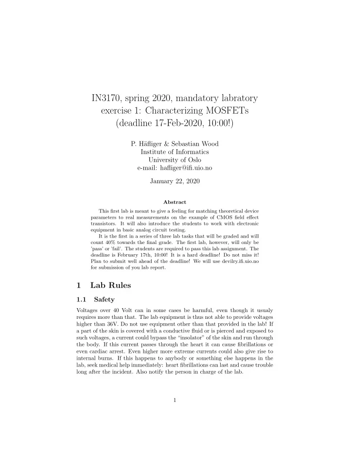
IN3170, spring 2020, mandatory labratory exercise 1: Characterizing MOSFETs (deadline 17-Feb-2020, 10:00!) P. H afliger & Sebastian Wood Institute of Informatics University of Oslo e-mail: hafliger@ifi.uio.no January 22, 2020 Abstract
IN3170, spring 2020, mandatory labratory exercise 1: Characterizing MOSFETs (deadline 17-Feb-2020, 10:00!) P. H¨ afliger & Sebastian Wood Institute of Informatics University of Oslo e-mail: hafliger@ifi.uio.no January 22, 2020 Abstract This first lab is meant to give a feeling for matching theoretical device parameters to real measurements on the example of CMOS field effect transistors. It will also introduce the students to work with electronic equipment in basic analog circuit testing. It is the first in a series of three lab tasks that will be graded and will count 40% towards the final grade. The first lab, however, will only be ’pass’ or ’fail’. The students are required to pass this lab assignment. The deadline is February 17th, 10:00! It is a hard deadline! Do not miss it! Plan to submit well ahead of the deadline! We will use devilry.ifi.uio.no for submission of you lab report. 1 Lab Rules 1.1 Safety Voltages over 40 Volt can in some cases be harmful, even though it usualy requires more than that. The lab equipment is thus not able to provide voltages higher than 36V. Do not use equipment other than that provided in the lab! If a part of the skin is covered with a conductive fluid or is pierced and exposed to such voltages, a current could bypass the “insolator” of the skin and run through the body. If this current passes through the heart it can cause fibrillations or even cardiac arrest. Even higher more extreme currents could also give rise to internal burns. If this happens to anybody or something else happens in the lab, seek medical help immediately: heart fibrillations can last and cause trouble long after the incident. Also notify the person in charge of the lab. 1
Some electronic components can explode if they are exposed to high currents. This is important to remember when working with electrolytic capacitors. How- ever, none of the capacitors provided in the lab are electrolytic capacitors. Never bring your own electronic components into the lab! 1.2 Conduct Good routines are necessary to make the work in the lab effective and safe: • Food and drinks are prohibited from every lab. • In general everybody is responsible for keeping the lab tidy. • Always turn off the power supply before you start adding and/or removing components. • Use an ESD protection wrist strap when handling ICs and other sensitive components.(ESD: electrostatic discharge) • Always clean up after using equipment and tools: – Turn off all equipment, except for lab computer. – Throw away cutoffs and vacuum clean the desk, chair, and floor if nessesary. – Place all components you have used back to their respective places. (Do this while you work, if you have a component you don’t use anymore, put it back.) • When you leave; the desk should be clean and ready for the next group. • Read the information posters in the lab describing what to do in case of fire or medical emergency. 2 Report and Group Assignments 2.1 Requirements for the Lab Report (read carefully!) You are required to execute the tasks and answer all the questions posed below and to submit a report on your work. The report needs to be explaining clearly what you have done, how you have done it, what the results were and what you conclude from them. Make sure to answer all questions! Supply the report with drawings of the circuits (including the values of the components and parameters you used where appropriate, e.g. bias voltages/currents, component sizes etc.) and measurement setups, and show your measurements in graphs! Use labels in the schematics that you draw, such as M 1 , M 2 (M is often used fro labelling CMOS transistors), opamp 1 , I 1 , V 1 etc. You should then use those labels in your text, since it is much easier to write: ’transistor M 1 in figure 1’ than ’the transistor third from the top and second from the left in the righthand side 2
circuit in figure 1’. MANDATORY : Include a photograph of your circuit into the report! 2.2 Graded Mandatory Group Assignments Note that this is part of the courses exam and strict rules apply as described in the document http://www.mn.uio.no/ifi/english/studies/admin/mandatory-assignments/ index.html . The page explains the significance of mandatory assignments in a course and in particular group assignments. It also specifies your responsibility to not plagiarize anybody else’s work and that you are required to conduct and understand your own experiments and obtain your own results, while you are still allowed and encouraged to exchange advice and experiences also between groups. Each group must deliver a written lab report using the Devilry online sub- mission system before the hard deadline indicated in the title. Note that you can submitt multiple times and the last submission before the deadline will be graded, so it might be a good idea to plan to submit preliminary versions well before the deadline. The points given for this lab assignment will determine if the lab assignment is accepted or rejected. You will need to pass this lab assigment in order to be admitted to the exam. The next two lab assignments will be weighted as 20% of the total score of the course, i.e. your final grade. Each task is labeled with how many points it will contribute towards the score. 3 Lab Task 3.1 Introduction The MOS transistor is the fundamental building block in microelectronics. De- pending on both usage and production the properties of the device varies sig- nificantly. During production the MOS transistor may be adapted to different settings like high voltage devices, high speed devices and analog devices and so on. In spite of this production flexibility, the major application of MOS transis- tors as switches in digital systems is setting the standard for devices available in silicon. Now, as digital systems are “moving out” interfacing directly with the real world through sensors and actuators (buzzword: cyberphysical systems), also analog interfacing functions must be included. A significant challenge is therefore to design high performance analog circuits in crude digital technology. The goal of this exercise is to characterize off-the-shelf MOS-FET transistors that we know very little about a-priory. We are going to use the ELVIS II board as a platform that provides a remov- able bread board to build your test circuits, built-in instruments for measuring electronic circuits (refered to as ’virtual instruments (VI)), and a convenient GUI on the computer to control those instruments. The ELVIS board has some limitations in functionality when it comes to automated measurements involv- ing multiple of those built-in instruments. In particular for this assignment, 3
there is no VI for characterizing MOSFETs. The name of the ’three wire cir- cuit analyzer’ sounds very promissing, but it is made for bipolar transistors and the controlling wire is current controlled to control the base current , while for MOSFETs we would need to control the voltage of the gate. The graphic programming language LabView offers the possibility to define new VIs your- self, but it’s not a very intuitive language (at least not to your lecturer). We’ll employ another fix for this lab, using the two wire analyzer and the variable voltage source and some creative wireing. 3.2 Tools • The NI-ELVIS bord and plug-in bread bord You shall use a bread board to plug in cables and discrete components to compose your test circuits. The bread bord can be removed from the socket in the ELVIS bord and each group can keep one for the duration of the course. Thus, once you are done for the day you can leave your components in place and lock your bord away or take it home with you until your next lab session. The ELVIS bord has some built in instruments that are displayed on the computer at each work place. You shall use those instruments to characterize your circuit. Some general advice: plan your layout of components and cables on the bread bord before you start plugging them in and try to make things compact and organized. • The NI ELVISmx Instrument Launcher BEFORE you launch the NI ELVISmx Instrument Launcher you should switch on the ELVIS board, such that the software (SW) recognizes the hardware (HW) correctly. Note that there are two power switches, one on the right hand side on the back of the board and one on top of th board also on the right near the back. You may launch the NI ELVISmx Instrument Launcher from the icon on your Windows desktop in the lab and you will get a list of icons representing the various instruments that are built in into the ELVIS board. See figure 1. Note that the interface looks now a bit more modern than in the description of IN1080. • The NI ELVISmx 2-wire VI Analyzer Another NI ELVISmx instrument i the 2-wire VI analyzer and when you click it its front panel pops up and looks as depicted in figure 2. It let’s you sweep a voltage and measure a current accross a device/circuit. The connections on the bread board left hand side between which you need to place your circuit under analysis are DUT+ and DUT- . For more help, press the ’help’ button. Note that this instrument will execute a series of measurements that you could have performed by hand. This is often a good thing, but has some pitfalls: you should know in some detail 4
Figure 1: The NI ELVISmx Instrument Launcher 5
Figure 2: The NI ELVISmx 2-wire VI Analyzer Virtual Instrument 6
Recommend
More recommend
Explore More Topics
Stay informed with curated content and fresh updates.
