I I I -V High-Electron Mobility Transistors on the path to THz - PowerPoint PPT Presentation
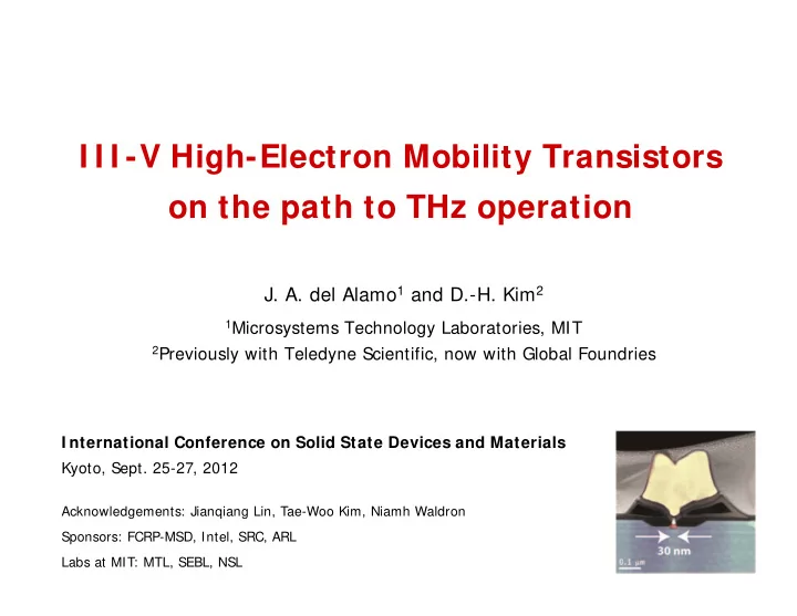
I I I -V High-Electron Mobility Transistors on the path to THz operation J. A. del Alamo 1 and D.-H. Kim 2 1 Microsystems Technology Laboratories, MIT 2 Previously with Teledyne Scientific, now with Global Foundries I nternational Conference on
I I I -V High-Electron Mobility Transistors on the path to THz operation J. A. del Alamo 1 and D.-H. Kim 2 1 Microsystems Technology Laboratories, MIT 2 Previously with Teledyne Scientific, now with Global Foundries I nternational Conference on Solid State Devices and Materials Kyoto, Sept. 25-27, 2012 Acknowledgements: Jianqiang Lin, Tae-Woo Kim, Niamh Waldron Sponsors: FCRP-MSD, Intel, SRC, ARL Labs at MIT: MTL, SEBL, NSL
Outline 1. High-frequency III-V HEMTs: megatrends 2. State-of-the-art InGaAs HEMTs and f T analysis 3. The path to THz operation 2
1. I I I -V HEMT: record f T vs. time Current record: f T =688 GHz f max =800 GHz Kim IEDM 2011 (Teledyne/MIT) (and MHEMT) • For >20 years, record f T obtained on InGaAs-channel HEMTs • InGaAs-channel HEMTs offer record balanced f T and f max 3
Record f T I I I -V HEMTs: megatrends • Over time: L g ↓ , In x Ga 1-x As channel x InAs ↑ • L g , x InAs saturated no more progress possible? 4
Record f T I I I -V HEMTs: megatrends • Over time: t ch ↓ , t ins ↓ • t ch , t ins saturated no more progress possible? 5
2. State-of-the-art I nGaAs HEMT L g =40 nm InGaAs MHEMT • In 0.7 Ga 0.3 As QW channel o t ch = 10 nm o n,Hall > 10,000 cm 2 /V-sec • In 0.52 Al 0.48 As barrier + In 0.7 Al 0.3 As spacer (Kim, EL 2011) Dual Si -doping (Kim, IEDM 2010) • • Pt (3 nm)/Ti/Pt/Au Schottky o t ins =4 nm • InP etch stop (t InP =6 nm) • L side =100 nm GaAs substrate • Gate stem > 250 nm Mo-based S/D with 2 m S-D spacing • Kim, IEDM 2011 6 6
TEM cross section Au Pt G S D Ti HEMT Epi Graded Buffer Buried Pt GaAs Substrate 7
Output and transfer characteristics Kim, IEDM 2011 1.2 3 L g =40 nm L g =40 nm V GS = 0.6 V 0.8 V 0.8 2 0.5 V I D [mA/ m] g m [mS/ m] 0.4 1 0.2 V V DS = 0.1 V 0.0 0 0.0 0.2 0.4 0.6 0.8 1.0 0.0 0.2 0.4 0.6 V DS [V] V GS [V] • Large current drive: I D >1 mA/µm at V DS =0.8 V • High transconductance: g mpk = 2.75 mS/ μ m at V DS =0.8 V • V T ≈ 0 V, R ON =280 Ω . μ m 8 8 8
High-frequency characteristics V DS =0.6 V, V GS =0.4 V 4 h 21 V DS =0.6 V, V GS =0.4 V 40 f T = 688 GHz 3 MSG f max = 800 GHz Gains [dB] 2 Stability Factor (k) U g 20 1 k 0 0 9 10 11 12 10 10 10 10 Frequency [Hz] • Only transistor of any kind with both f T and f max > 680 GHz • Obtained at same bias point, V DS =0.6 V Kim, IEDM 2011 9 9
f T vs. f max 300 600 700 = f avg = f f 1500 m ax Kim, IEDM 2010 (f max =1.25 GHz) 1000 f max [GHz] TSC/MIT Kim, IEDM 2011 (This work) MIT/TSC HEMT 500 Fujitsu HEMT NGAS HEMT SNU HEMT UCSB HBT UIUC HBT TSC HBT HRL HBT ETH HBT 0 0 200 400 600 800 1000 f T [GHz] • Record f T FET • Best-balanced f T and f max transistor 10
f t analysis G S D C gs C gd g mi v gs R S R D g oi • First-order f T expression for HEMT: 11 11
Break out extrinsic capacitances G S D • Capacitance components: 12 12
Delay time analysis • Delay time: • Components of delay time: Intrinsic delay (transit time) Extrinsic delay Parasitic delay 13 13
Delay components of L g = 40 nm I nGaAs HEMT Delay time from f T : ~231 fs yields <v e >=5x10 7 cm/s • Intrinsic delay: ~81 fs • Extrinsic delay: ~99 fs most significant • Parasitic delay: ~50 fs • Unaccounted: ~9 fs 14 14
Scaling of delay components 600 V DS = 0.6 V Transit V GS - V T = 0.3V 400 Delays [fs] 200 ext par 0 0 100 200 L g [nm] ext and par do not scale, become dominant for L g < 50 nm 15 15
Scaling of small-signal components V DS = 0.6 V V GS - V T = 0.3V 2000 C gs C gs , C gd [fF/mm] C gs_ext 1000 C gd_ext C gd 0 0 100 200 L g [nm] As L g ↓: do not scale do not scale ↑ ↓ 16 16
3. The path to THz operation • Intrinsic delay ↓ L g ↓ • Extrinsic delay ↓ : C gsext , C gdext ↓ gate engineering g mi ↑ harmonious scaling • Parasitic delay ↓ : R S +R D ↓ S/D engineering g oi /g mi ↓ harmonious scaling 17 17
How to reach f t = 1 THz? 1200 30% reduction 1 THz 1000 in all the parasitics 800 600 f T [GHz] 400 V DS = 0.6 V Measured f T Modeled f T Model Projection 200 30 100 L g [nm] f T = 1 THz feasible by: scaling to L g ≈ 25 nm ~30% parasitic reduction 18 18
Approach to R S + R D ↓ : self-aligned process Kim, IEDM 2010 Waldron, TED 2010 1.0 VGS = 0.5 V L g =50 nm L side =100 nm 0.4 V 0.8 0.3 V 0.6 I D [mA/ m] 0.2 V 0.4 0.1 V 0.2 0 V 0.0 0.0 0.1 0.2 0.3 0.4 0.5 0.6 0.7 V DS [V] • Dry-etched Mo contacts: R c = 7 Ω . μ m • L g =50 nm, R ON =290 Ω . μ m, g mpk =2.2 mS/ μ m @ V DS =0.5 V 19
L g = 60 nm self-aligned I n 0.7 Ga 0.3 As HEMT L g =60 nm 4 Measured data Modeled data V GS = 0.2 V, V DS = 0.6 V H 21 40 H 21 , MAG/MSG and U g [dB] 3 f T =595 GHz f max =680 GHz U g 2 K 20 MAG/MSG 1 K 0 0 1 10 100 1000 Frequency [GHz] Kim, IEDM 2010 Highest f T and f max of any FET at L g 60 nm 20
L g = 30 nm self-aligned I nGaAs MOSFET with L side ~ 30 nm Lin, IEDM 2012 V gs = -0.2 to 0.5 V in 0.1 V step 600 R on =475 m (at V gs =0.7 V) L g = 30 nm I d ( A/ m) 400 200 0 0.0 0.1 0.2 0.3 0.4 0.5 V ds (V) L side ~30 nm g mpk =1.4 mS/ μ m R ON =475 Ω .µm access region design critical! 21
Regrown source and drain regions L ch =55 nm InGaAs MOSFET: R ON =199 Ω .µm Egard, IEDM 2011 L ch =30 nm InGaAs MOSFET: R ON =133 Ω .µm Zhou, EDL 2012 22
Harmonious scaling: aspect ratio of record f t devices Channel Aspect Ratio: L g /t ch Insulator Aspect Ratio: L g /t ins Dimensions verified by XTEM • Channel AR : 3 ~ 4 For L g =25 nm • Insulator AR: 7 ~ 10 t ch ~ 7 nm, t ins ~ 3 nm 23 23
Limit to HEMT barrier scaling: gate leakage current InAlAs/InGaAs HEMTs V DS =0.5 V At L g =30 nm, modern HEMTs are at the limit of scaling! 24 24
Limit to HEMT barrier scaling: gate leakage current InAlAs/InGaAs HEMTs 10 -5 x! Al 2 O 3 (3 nm)/InP (2 nm)/InGaAs MOSFET V DS =0.5 V Need high-K gate dielectric: HEMT MOSFET! 25 25
I I I -V MOSFET: deep scaling possible InP (1 nm) + Al 2 O 3 (0.4 nm) + HfO 2 (2 nm) EOT ~ 0.9 nm [ vs. 4 nm InAlAs EOT = 1.3 nm] Equivalent oxide should bring us to L g =20 nm thickness V ds =0.5 and 0.05 V -6 10 L g = 300 m Long-channel -7 10 I d (A/ m) In 0.53 Ga 0.47 As MOSFET -8 10 μ e ≈ 2700 cm 2 /V.s -9 10 S=69 mV/dec -10 10 Lin, IEDM 2012 -11 10 -0.2 0.0 0.2 0.4 0.6 V gs (V) S=69 mV/dec Low D it at MOS interface demonstrated 26
High-frequency I nGaAs MOSFETs L g =100 nm InGaAs MOSFET with L side ~5 nm, EOT=1.9 nm Kim, VLSI Tech 2012 L g =100 nm μ e =4600 cm 2 /V.s f t =245 GHz, R ON =323 Ω .µm, g m =1.7 mS/µm, S=105 mV/dec 27
THz MOSFETs: possible designs n + n + Etched S/D QW-MOSFET Regrown S/D QW-MOSFET Gate-all-around FinFET nanowire FET 28
Conclusions • THz III-V FETs just around the corner need to reduce parasitics need to scale harmoniously • Exploding interest on III-V CMOS: huge opportunity for THz III-V electronics! fast technology progress new processes and tools fundamental research on transport, interface, etc. Si as substrate for THz electronics 29 29
Recommend
More recommend
Explore More Topics
Stay informed with curated content and fresh updates.
