MTLE-6120: Advanced Electronic Properties of Materials Semiconductor - PowerPoint PPT Presentation
1 MTLE-6120: Advanced Electronic Properties of Materials Semiconductor transistors for logic and memory Contents: Aside: vacuum tubes Bipolar junction transistors (BJT) Junction field effect transistors (JFET) Metal oxide
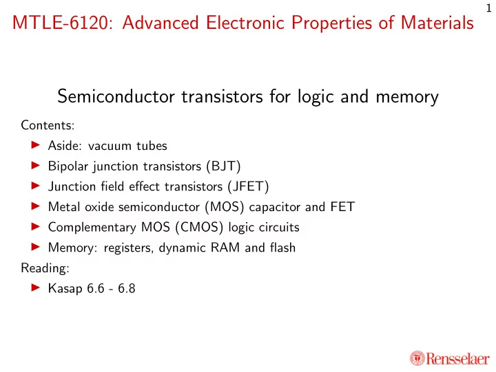
1 MTLE-6120: Advanced Electronic Properties of Materials Semiconductor transistors for logic and memory Contents: ◮ Aside: vacuum tubes ◮ Bipolar junction transistors (BJT) ◮ Junction field effect transistors (JFET) ◮ Metal oxide semiconductor (MOS) capacitor and FET ◮ Complementary MOS (CMOS) logic circuits ◮ Memory: registers, dynamic RAM and flash Reading: ◮ Kasap 6.6 - 6.8
2 Vacuum tube diodes ◮ Thermionic emission from cathode ◮ Electrons collected at anode with positive bias ◮ Anode not heated: cannot emit electrons ⇒ no reverse current ◮ Nominally similar characteristics to pn -junction diode Images: Wiki: Vacuum tubes
3 Vacuum tube triodes ◮ Control plate / grid between cathode and anode ◮ Negative bias repels electrons; reduces current ◮ Small changes in voltage ⇒ large changes in current ◮ Acts as a switch or amplifier Images: Wiki: Vacuum tubes
4 Vacuum tube computers ◮ Each triode in own separate tube ◮ ENIAC computer in 1946: 17468 such tubes ◮ Key characteristic required: three terminal device where third terminal controls current between first two ◮ In principle: computer made entirely of hydrualically or pneumatically-controlled valves! Images: Wiki: Vacuum tubes
5 Bipolar Junction Transistor (BJT) ◮ Heavily doped emitter E (like cathode in triode) ◮ Thin lightly-doped base B (like control plate / grid) ◮ Lightly-doped collector C (like anode) ◮ Either pnp (shown above) or npn (polarities reversed) ◮ Which one does the vacuum tube triode correspond to?
6 BJT: junction potentials ◮ Two pn -junctions: E-B and C-B ◮ Normal (active) operation: forward-bias E-B and reverse-bias C-B ◮ E-B junction: depletion region mostly in base ◮ C-B junction: comparitively symmetrical ◮ Potential drop across depletion regions; negligible field in interiors ◮ Hole concentration at B-end of E-B junction: p n (0) = n 2 N d exp eV EB i k B T ◮ Hole concentration at B-end of C-B junction: p n ( W B ) ≈ 0
7 BJT: current flow W B = eAD h n 2 ◮ Diffusion current across base: I E ≈ I C = eAD h p n 0 N d W B exp eV EB i k B T ◮ Current out of n -type base has to be electrons: two factors in α ≡ I C /I E ◮ Electron current in E-B: small due to asymmetric doping γ = 1 NdWBµe 1+ NaWE µh ◮ Recombination: small for thin lightly-doped base α T = 1 − W 2 B / (2 D h ) τ h ◮ Current transfer ratio α = γα T � 0 . 99 for typical BJTs 1 − α ∼ 10 2 − 10 3 ◮ Current gain β ≡ I C /I B = α
8 BJT: IV characteristics ◮ Ideal characteristic: I C = I E independent of V CB ◮ Leakage current in reverse-biased C-B junction, I CB 0 ◮ At high V CB , I C = αI E + I CB 0 and I B = (1 − α ) I E − I CB 0 ◮ But slope of I C vs V CB increases for finite I E (beyond I CB 0 ) ◮ Early effect: C-B depletion width increases with V CB ◮ This reduces W B , making hole diffusion easier, and therefore I E ↑
9 BJT: common base amplifier ◮ Small changes in E-B potential strongly affect I C ≈ I E = I E 0 exp eV EB k B T ◮ Convert ‘amplified’ current to voltage using resistor ◮ Collector potential V CB = − V CC + R C I C ◮ Voltage gain (controlled by selecting I E and R C ): ∂V CB ∂I C = I E R C = R C ∂V EB ∂V EB k B T
10 BJT: common emitter amplifier ◮ Note npn -transistor: polarities reversed ◮ Current amplifier: input I B amplified by β to output I C ◮ With leakage current, I B = (1 − α ) I E − I CB 0 and I C = I E − I B = βI B + I CB 0 1 − α � �� � I CE 0 ◮ Operate at V CE > V BE , else saturation: I C limited by I E
11 Junction Field-effect Transistor (JFET) ◮ n -JFET: narrow n channel between p + gates (reversed for p -JFET) ◮ Width of n channel determined by depletion regions ◮ Basic idea: control channel width and conduction using gates ◮ Always operate with channel potential > gate ⇒ reverse bias
12 JFET: channel IV characteristics ◮ First consider applied V DS with V GS = 0 ◮ Voltage of channel-gate junction increases from S to D ◮ Correspondingly increasing depletion width narrows channel ◮ Increase V DS , current I D increases, but channel narrows ◮ At V sat DS , channel pinches off at D end, I D saturates
13 JFET: gate effects ◮ Apply negative gate potential: V DG increases ◮ Narrower depletion region, earlier pinch off ◮ V sat DS = V P + V GS , where pinchoff voltage V P = V sat DS at V GS = 0 ◮ Therefore, gate potential controls channel current and effective resistance ◮ Strong-enough V GS shuts off channel completely ⇒ V off GS � � 2 ◮ Empirical behaviour: I DS = I DSS 1 − V GS /V off GS
14 JFET amplifier ◮ Amplifier: gate voltage controls channel current ◮ Convert channel current to voltage through resistor R D ◮ Vaguely similar to common-emitter amplifier ◮ Set operating ‘quiescent’ point at center of operating range ◮ Signal amplitudes small enough to stay in range ◮ Voltage gain � � ∂V DS = R D ∂I DS = 2 I DSS R D 1 − V GS ∂V GS ∂V GS V off V off GS GS
15 Metal-oxide-semiconductor (MOS) capacitor Metal Oxide Semiconductor Metal Oxide Semiconductor Metal Oxide Semiconductor ◮ Metal and SC separated by an insulating oxide: why don’t the bands bend? ◮ Apply potential: linear variation in oxide, typical bending in SC ◮ Vacuum level (potential) continuous, D ⊥ continuous ◮ For p -SC and positive V metal , CB bends towards E F ◮ For V metal > V th (threshold), CB closer than VB to E F ◮ Inversion region: n > p in p -type semiconductor ◮ Analogous case with reversed potentials for n -type semiconductors
16 Metal-Oxide-SC Field-effect Transistor (MOSFET) ◮ Enhancement n -channel MOSFET: metal- p capacitor surrounded by n + ◮ MOS inversion: generates an n channel at surface ◮ Comparison with n -JFET: existing channel suppressed by gate junction ◮ Analogous depletion n -MOSFET: replace p above with light n ◮ Flip n ↔ p and polarities ⇒ enhancement and depletion p -MOSFETs
17 MOSFET: gate response ◮ For V GS < V th , n + contacts separated by depletion layer ◮ No channel ⇒ I D = 0 irrespective of V DS ◮ One V GS > V th , inversion layer forms an n -channel ◮ For low V DS , channel behaves like an Ohmic resistor
18 MOSFET: drain response ◮ Increasing V DS causes reduction in V GD ◮ Channel begins to narrow near drain; current starts to level off ◮ At V DS = V sat DS = V GS − V th , channel pinches off at drain end ◮ Beyond this potential, I D does not increase with increasing V DS
19 MOSFET: IV characteristics ◮ Saturation drain voltage V sat DS = V GS − V th ◮ Saturation drain current I DS = K ( V GS − V th ) 2 (1 + λV DS ) ◮ Coefficient K ∼ Cµ e 2 L 2 , where C = MOS capacitance, L = channel length ◮ Coefficient λ due to Early effect (exactly like in BJT, JFET) ◮ Similar characteristics to JFET ⇒ similar amplifier circuits ◮ Switching: V GS > V th ⇒ R DS small (on) vs V GS < V th ⇒ R DS large (off) ◮ On-off ratio R off DS /R on DS , switching time ∼ RC
20 Complementary MOS (CMOS) logic ◮ Complementary MOS: combine p and n -MOS transistors ◮ Inverter / NOT gate: V in < V th ⇒ V out = V dd , V in > V th ⇒ V out = V ss ◮ Digital logic: for input 0 and 1, output 1 and 0 respectively ◮ NOR (NOT OR) gate: output 0 (NOT 1) if any input 1 ◮ NAND (NOT AND) gate: output 0 (NOT 1) if all inputs 1 ◮ Any logic or arithmetic operation using just three gates!
21 Arithmetic circuits ◮ XOR (exclusive OR) gate: output 1 if exactly one input 1 ◮ 1-bit adder: sum bit = XOR, carry bit = AND ◮ 8-bit adder: chain bit additions together ◮ N -bit adder: requires ∝ N log 2 N gates ◮ N -bit multiplier: adder of N numbers with N -bits each
22 Example: Xeon Phi 7210 ◮ 64 compute cores ◮ Each core: 8 × 64-bit multipliers ◮ Net: 10 12 64-bit math operations per second ◮ 8 × 10 9 CMOS transistors in 8 cm 2 of Si!
23 Bistable latches (flip-flops) ◮ When R = S = 0 : latch stores previous value ◮ Feedback loop between two inverters ◮ S = 1 sets value to 1, R = 1 resets it to 0 ◮ Volatile memory: data lost when circuit powered off ◮ Mechanism used in registers and static RAM ◮ Minimum 8 transistors / bit as shown above (low-density, high power)
24 Dynamic RAM ◮ Bit = whether capacitor is charged ◮ Transistor in off state: capacitor isolated; retains charge ◮ To read, transistor in specific row and column switched on ◮ Reading destroys state; must be written back ◮ State lost due to leakage ⇒ refresh circuitry ◮ Volatile: charge retention only ∼ 100 ms ◮ 1 transistor / bit: high-density, low power ◮ 8GB DDR4 memory: 8 × 10 9 transistors in < 10 cm 2 Si
25 Flash memory / SSD: floating-gate transistors ◮ Floating gate transistor: bit = whether floating gate is charged ◮ Charge on floating gate affects V th ◮ Read bit by checking if transistor is on at specified V GS ◮ Write bit by hot-electron injection from channel ◮ Erase bit by Fowler-Nordheim tunneling to upper gate ◮ NOR-flash: closer to random-access; erase only in large blocks ◮ NAND-flash: all access in large pages / blocks (eg. SSD)
Recommend
More recommend
Explore More Topics
Stay informed with curated content and fresh updates.
