EE-612: Lecture 26: CMOS Limits Mark Lundstrom Electrical and - PowerPoint PPT Presentation
EE-612: Lecture 26: CMOS Limits Mark Lundstrom Electrical and Computer Engineering Purdue University West Lafayette, IN USA Fall 2006 NCN www.nanohub.org Lundstrom EE-612 F06 1 Outline 1) Review: CMOS Metrics 2) MOSFET limits 3)
EE-612: Lecture 26: CMOS Limits Mark Lundstrom Electrical and Computer Engineering Purdue University West Lafayette, IN USA Fall 2006 NCN www.nanohub.org Lundstrom EE-612 F06 1
Outline 1) Review: CMOS Metrics 2) MOSFET limits 3) Circuit limits 4) System Limits Lundstrom EE-612 F06 2
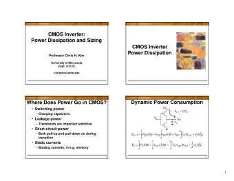
CMOS metrics E S = 1 1) Switching energy: 2 2 CV DD τ S = CV DD 2) Switching delay: I D (ON) D = α f CV DD 2 3) Dynamic power: P C 2 V DD 3 E S τ = 1 4) Energy-delay product: 2 I D (on) Lundstrom EE-612 F06 3
Outline 1) CMOS Metrics 2) MOSFET limits 3) Circuit limits 4) System limits Lundstrom EE-612 F06 4
device limit questions 1) minimum energy dissipation per logic transition 2) minimum channel length 3) maximum device density 4) minimum device delay 5) power density 6) power-limited device density 7) CMOS vs. the ultimate switch Lundstrom EE-612 F06 5
acknowledgment The approach that I take here is similar to the work of V.V. Zhirnov, R.K. Cavin, J.A. Hutchby, and G. Bourianoff, “Limits to Binary Logic Switch Scaling - A Gedankan Model,” Proc. IEEE , Special Issue on Nanoelectronics and Nanoscale Processing, Nov. 2003. Lundstrom EE-612 F06 6
MOSFETs control current with potential barriers electron energy vs. position S G D V D ≈ 0V V GS I D V D = V DD V DS E.O. Johnson, RCA Review , 1971 Lundstrom EE-612 F06 7
ultimate MOSFET in the off-state low gate voltage: OFF state large barrier L E C E B E F E D source (strong scattering) E F − qV DS ballistic channel drain (strong scattering) y Lundstrom EE-612 F06 8
ultimate MOSFET in the on-state ON state L E C high gate voltage: no barrier E B = 0 E F source (strong scattering) E D (on) E F − qV DS ballistic channel drain (strong scattering) y Lundstrom EE-612 F06 9
minimum switching energy To distinguish off from on , electrons in the source must have less than a 50:50 chance of moving over the barrier from the source to drain. OFF E C e − E B / k B T < 1 E B 2 source L E B > E min = k B T ln(2) drain y Lundstrom EE-612 F06 10
minimum switching energy (ii) To distinguish on from off , electrons in the drain must have less than a 50:50 chance of moving over the barrier from the drain to source. e − E D / k B T < 1 ON E C 2 E D > E min = k B T ln(2) source E D L drain y E S > k B T ln(2) = 0.003 aJ (minimum energy dissipation per logic transition) Lundstrom EE-612 F06 11
minimum switching energy (iii) Does it take additional energy to move the gate-controlled barrier up and down? ? ON E C + 1 2 2 C TOT V DD I V in ( t ) - source E D L drain y ( k B T ln(2) is the min energy dissipation per logic transition) Lundstrom EE-612 F06 12
minimum device size To distinguish off from on , the probability that an electron tunnels through the barrier must be less than a 50:50. ⎛ ⎞ P (WKB) = exp − 2 2 mE ⎟ < 1 ⎜ L � ⎝ ⎠ 2 “OFF” E C � L > ln(2) 2 source 2 mE L drain E = k B T = E S (min) ln(2) y h L min ≈ = 1.5nm(300K) 2 mE S (min) Lundstrom EE-612 F06 13
minimum device size (again) Δ p Δ x > h Δ p 2 ( ) “OFF” E C 2 m = E S min source L Δ x = L drain h y L min ≈ = 1.5nm(300K) 2 mE S (min) Lundstrom EE-612 F06 14
minimum device size (iii) Note also that the size of a device, S , must be larger than the size of its minimum element, L . (For a MOSFET, S ~ 10-15 L .) Lundstrom EE-612 F06 15
maximum device density 1 2 = 4.7 × 10 11 cm -2 n D (max) ≈ ( ) 10 L min We will show later that device density is limited by the maximum power density that can be dissipated - not by device size. Lundstrom EE-612 F06 16
maximum device speed The minimum device transit time sets the maximum speed. t s ≈ L t S (min) ≈ L min L min = υ υ 2 E m ON E C E = k B T = E S (min) ln(2) source L h L min ≈ drain y 2 mE S (min) h t S (min) ≈ E S (min) = 0.04 ps (300K) Δ E Δ t = � Lundstrom EE-612 F06 17
power dissipation D = α n D E S P t S α = 1, n D (max), E S (min), t S (min) D = 3.7 × 10 4 W/cm 2 P 6 × 10 3 W/cm 2 surface of the sun: forced water cooling: < 800 W/cm 2 ITRS: < 100 W/cm 2 Lundstrom EE-612 F06 18
power-limited device density maximum power dissipation per unit area limits density - not our ability to make devices small. n D (max) = P max t S (min) ˆ α E S (min) max = 100W/cm 2 and α = 1 for P n D (max) ~ 1.5 × 10 9 devices/cm 2 ˆ Lundstrom EE-612 F06 19
power-constrained design P standby max = 100W/cm 2 P power there is an optimum device size! P active integration density (Dave Frank, IBM) Lundstrom EE-612 F06 20
power-delay product D τ = E S t S = E S P t S D τ min = E S min = k B T ln2 P But….this metric does not capture the fact that we usually want to runs circuits fast and at low power. Lundstrom EE-612 F06 21
energy-delay product h E τ min = E S t S min = E S (min) E S (min) = h ( ) Δ E Δ t > h Lundstrom EE-612 F06 22
summary E S > k B T ln(2) 1) Switching energy: t S > h E S (min) 2) Switching delay: L min > h 3) Device size: 2 mE S (min) n D < P 4) Device density: ˆ max t S (min) E S (min) E τ > h 5) Energy-delay: Lundstrom EE-612 F06 23
comparison to 65nm CMOS parameter 65nm ITRS Limit 65nm /Limit E s (aJ) 23 0.003 8000 τ ( fs) 640 40 16 L (nm) 25 nm 1.5 nm 17 S (cm − 2 ) 0.8 x 10 9 1.5 x 10 9 0.5 ˆ n 1.1 x 10 -34 136,000 E τ (J-s) 1.5 x 10 -29 Lundstrom EE-612 F06 24
outline 1) CMOS Metrics 2) MOSFET limits 3) Circuit limits 4) System limits Lundstrom EE-612 F06 25
minimum V DD V DD S V DD V OUT --> D V DD /2 V IN V OUT D V DD V DD /2 S V IN --> Question: What is the smallest V DD for a CMOS inverter? Answer: The smallest V DD that gives a gain > 1 Lundstrom EE-612 F06 26
reference J.D. Meindl and J.A. Davis, “ The Fundamental Limit on Binary Switchin Energy for Terascale Integration, IEEE J. Solid-State Circuits , 35 , pp. 1515-1516, 2000. Lundstrom EE-612 F06 27
minimum V DD V DD assume subthreshold operation: S ( ) ( ) / mk B T 1 − e − qV DS / k B T q V GS − V T I D = Ke D V IN V OUT ( ) ( ) / mk B T 1 − e − qV out / k B T q V in − V TN I DN = K N e D ( ) ( ) / mk B T 1 − e ( ) / k B T q V DD − V in + V TP q V out − V DD I DP = K P e S ( ) I DN = I DP → V out V in Lundstrom EE-612 F06 28
minimum V DD (ii) ( ) ( ) = K P e ( ) / mk B T 1 − e − qV out / k B T ( ) / mk B T 1 − e ( ) / k B T q V in − V TN q V DD − V in + V TP q V out − V DD K N e K N = K P = K A V = dV out ( ) V TN = V T = − V TP = f V DD solve for dV in m = 1 ( ) k B T A V > 1 ⇒ V DD > 2ln 2 q ( ) k B T V DD min = 2ln 2 q Lundstrom EE-612 F06 29
minimum V DD (iii) e − E D / k B T < 1 E D > E D min = k B T ln(2) 2 ON E C V DD min = E D min / q = k b T ( ) q ln 2 source E D L drain 2 MOSFETS in series ⇒ y ( ) k B T V DD min = 2ln 2 q Lundstrom EE-612 F06 30
minimum switching energy E S = 1 V DD min = 2ln(2) k B T / q 2 2 C TOT V DD S E S = 1 2 QV DD D V OUT Q min = q V IN + D E S = 1 C TOT 2 Q min V DD min - S E S = k B T ln(2) Lundstrom EE-612 F06 31
outline 1) CMOS Metrics 2) MOSFET limits 3) Circuit limits 4) System limits Lundstrom EE-612 F06 32
circuit performance device CPU circuit increase delay: ~ 400 × 0.64 ps 250 ps ~300 × switching 23 aJ 6000 aJ energy: ~ 10 − 29 J-s ~ 10 − 24 J-s ~100,000 × energy- delay: Lundstrom EE-612 F06 33
circuits and fundamental limits parameter CPU circuit Limit circuit /limit E s (aJ) 6000 0.003 2,000,000 τ ( fs) 250,000 40 6250 E τ (J-s) 1.4 x 10 -24 1.1 x 10 -34 ~10 10 Since 1960, switching energy has decreased by about 5 orders of magnitude. (J.D. Meindl, Q. Chen, and J.A. Davis, “Limits on Silicon Nanoelectronics for Terascale Integration,” Science , 239 , pp. 2044- 2049, 2001) Lundstrom EE-612 F06 34
chip performance index B = N ops / cm 2 -s τ S CPI = N 1 = N × ops / s-cm 2 -W ( ) τ S E S t S E S CPI : 10 23 (today’s high-performance logic) CPI ultimat : 10 32 (since 1960, the CPI has increased by factor of ~ 10 14 ) J.D. Meindl, “Low Power Microelectronics: Retrospect and Prospect,” Proc. IEEE , 83 , 619-635, 1995 Lundstrom EE-612 F06 35
summary 1) Key device metrics include size, switching energy, and speed. 2) Key system metrics include density, switching energy, speed, and power. 3) Device metrics are ‘approaching’ fundamental limits. 4) System metrics are a long way from fundamental limits. Lundstrom EE-612 F06 36
outline 1) CMOS Metrics 2) MOSFET limits 3) Circuit limits 4) System limits Lundstrom EE-612 F06 37
Recommend
More recommend
Explore More Topics
Stay informed with curated content and fresh updates.
